![]()
Manufacturing
LOW-COST
Silicon Carbide Epi/Wafers

Company
TrueNano, Inc. is an R&D company located in Westminster, CO. It develops a select number of semiconductor-based material and device technologies for efficient power convertors, invertors, and variable frequency converters. Applications include electric vehicles, solar invertors, and a wide range of electrified electromechanical systems.
Technology
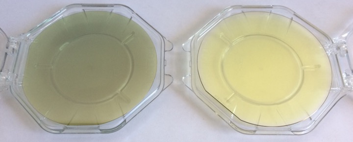
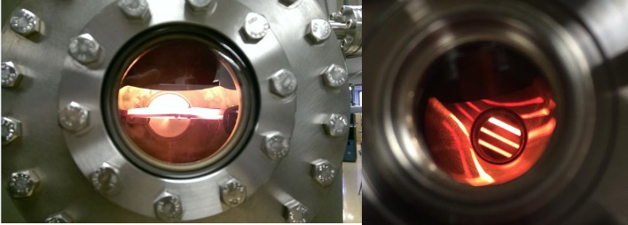
TrueNano Inc. is developing cost effective silicon carbide epi-layers and wafers using its patented Hot Filament Chemical Vapor Deposition process (HFCVD). HFCVD has all the advantages of a CVD process (low cost precursors and continuous growth) and the additional degrees of freedom from the hot filament, namely preconditioning of process gases and independent temperature control, enabling lower growth temperatures while maintaining high growth rate.
News
09/13/2022 - TeNano, Inc. in collaboration with the University of Colorado, Boulder presented a paper entitled "3C-SiC Island Growth on 4H-SiC Terraces" at the International Conference on Silicon Carbide and Related Material in Davos, Switzerland.
11/13/2019 - TrueNano, Inc. has been awarded a Navy Phase II STTR grant aimed at the growth of Silicon Carbide on 6 and 8 inch substrates. This work is performed in collaboration with the University of Colorado, Boulder.
09/30/2019 - TrueNano, Inc. in collaboration with the University of Colorado, Boulder presented a paper entitled "Analysis of Defect-Free Hot Filament CVD-grown 3C-SiC" at the International Conference on Silicon Carbide and Related Materials in Kyoto, Japan.
04/18/2018 - TrueNano, Inc. has been awarded a Navy Phase I STTR grant aimed at the growth of Silicon Carbide on 6 and 8 inch substrates.
Contact
TrueNano, Inc.
10850 Dover St. Suite 500
Westminster, CO 80021
USA
info@truenano.com