The ideal transistor model is based on the ideal p-n diode model and provides a first-order calculation of the dc parameters of a bipolar junction transistor. To further simplify this model, we will assume that all quasi-neutral regions in the device are much smaller than the minority-carrier diffusion lengths in these regions, so that the "short" diode expressions apply. The use of the ideal p-n diode model implies that no recombination within the depletion regions is taken into account. Such recombination current will be discussed in section 5.4.2. |
The discussion of the ideal transistor starts with a discussion of the forward active mode of operation, followed by a general description of the four different bias modes, the corresponding Ebers-Moll model and a calculation of the collector-emitter voltage when the device is biased in saturation. |
5.3.1. Forward active mode of operation |   |
The forward active mode is obtained by forward-biasing the base-emitter junction. In addition we eliminate the base-collector junction current by setting VBC = 0. The minority-carrier distribution in the quasi-neutral regions of the bipolar transistor, as shown in Figure 5.3.1, is used to analyze this situation in more detail. |
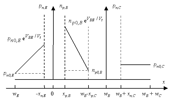 |
| Figure 5.3.1. : | Minority-carrier distribution in the quasi-neutral regions of a bipolar transistor (a) Forward active bias mode. (b) Saturation mode. |
The values of the minority carrier densities at the edges of the depletion regions are indicated on the Figure 5.3.1. The carrier densities vary linearly between the boundary values as expected when using the assumption that no significant recombination takes place in the quasi-neutral regions. The minority carrier densities on both sides of the base-collector depletion region equal the thermal equilibrium values since VBC was set to zero. While this boundary condition is mathematically equivalent to that of an ideal contact, there is an important difference. The minority carriers arriving at x = wB - xp,BC do not recombine. Instead, they drift through the base-collector depletion region and end up as majority carriers in the collector region. |
The emitter current due to electrons and holes are obtained using the "short" diode expressions derived in section 4.4.2.5, yielding: |
 | (5.3.1) |
and |
 | (5.3.2) |
It is convenient to rewrite the emitter current due to electrons, IE,n, as a function of the total excess minority charge in the base, DQn,B. This charge is proportional to the triangular area in the quasi-neutral base as shown in Figure 5.3.1 a) and is calculated from: |
 | (5.3.3) |
which for a "short" diode becomes: |
 | (5.3.4) |
And the emitter current due to electrons, IE,n, simplifies to: |
 | (5.3.5) |
where tr is the average time the minority carriers spend in the base layer, i.e. the transit time. The emitter current therefore equals the excess minority carrier charge present in the base region, divided by the time this charge spends in the base. This and other similar relations will be used to construct the charge control model of the bipolar junction transistor in section 5.6.2. |
A combination of equations (5.3.1), (5.3.4) and (5.3.5) yields the transit time as a function of the quasi-neutral layer width, wB', and the electron diffusion constant in the base, Dn,B. |
 | (5.3.6) |
We now turn our attention to the recombination current in the quasi-neutral base and obtain it from the continuity equation (2.9.3): |
 | (5.3.7) |
By applying it to the quasi-neutral base region and assuming steady state conditions: |
 | (5.3.8) |
which in turn can be written as a function of the excess minority carrier charge, DQn,B, using equation (5.3.3). |
 | (5.3.9) |
Next, we need to find the emitter efficiency and base transport factor. The emitter efficiency defined by equation (5.2.17), becomes: |
 | (5.3.10) |
It is typically the emitter efficiency, which limits the current gain in transistors made of silicon or germanium. The long minority-carrier lifetime and the long diffusion lengths in those materials justify the exclusion of recombination in the base or the depletion layer. The resulting current gain, under such conditions, is: |
 | (5.3.11) |
From this equation, we conclude that the current gain can be larger than one if the emitter doping is much larger than the base doping. A typical current gain for a silicon bipolar transistor is 50 - 150. |
The base transport factor, as defined in equation (5.2.18), equals: |
 | (5.3.12) |
This expression is only valid if the base transport factor is very close to one, since it was derived using the “short-diode” carrier distribution. This base transport factor can also be expressed in function of the diffusion length in the base: |
 | (5.3.13) |
| Example 5.2 | Consider a pnp bipolar transistor with emitter doping of 1018 cm-3 and base doping of 1017 cm-3. The quasi-neutral region width in the emitter is 1 mm and 0.2 mm in the base. Use mn = 1000 cm2/V-s and mp = 300 cm2/V-s . The minority carrier lifetime in the base is 10 ns. Calculate the emitter efficiency, the base transport factor, and the current gain of the transistor biased in the forward active mode. Assume there is no recombination in the depletion region. |
| Solution | The emitter efficiency is obtained from:
The base transport factor equals:
The current gain then becomes:
where the transport factor, a, was calculated as the product of the emitter efficiency and the base transport factor:
|
5.3.2. General bias modes of a bipolar transistor | |
While the forward active mode of operation is the most useful bias mode when using a bipolar junction transistor as an amplifier, one cannot ignore the other bias modes especially when using the device as a digital switch. All possible bias modes are illustrated with Figure 5.3.2. They are the forward active mode of operation, the reverse active mode of operation, the saturation mode and the cut-off mode. |
 |
| Figure 5.3.2.: | Possible bias modes of operation of a bipolar junction transistor. |
The forward active mode is the one where we forward bias the base-emitter junction, VBE > 0 and reverse bias the base-collector junction, VBC < 0. This mode, as discussed in section 5.3.1, is the one used in bipolar transistor amplifiers. In bipolar transistor logic circuits, one frequently switches the transistor from the “off” state to the low resistance “on” state. This “off” state is the cut-off mode and the “on” state is the saturation mode. In the cut-off mode, both junctions are reversed biased, VBE < 0 and VBC < 0, so that very little current goes through the device. This corresponds to the “off” state of the device. In the saturation mode, both junctions are forward biased, VBE > 0 and VCB > 0. This corresponds to the low resistance “on” state of the transistor. |
Finally, there is the reverse active mode of operation. In the reverse active mode, we reverse the function of the emitter and the collector. We reverse bias the base-emitter junction and forward bias the base-collector junction, or VBE < 0 and VBC > 0. In this mode, the transistor has an emitter efficiency and base transport factor as described by equations ((5.3.10) and (5.3.12), where we replace the emitter parameters by the collector parameters. Most transistors, however, have poor emitter efficiency under reverse active bias since the collector doping density is typically much less than the base doping density to ensure high base-collector breakdown voltages. In addition, the collector-base area is typically larger than the emitter-base area, so that even fewer electrons make it from the collector into the emitter. |
Having described the forward active mode of operation, there remains the saturation mode, which needs further discussion. Cut-off requires little further analysis, while the reverse active mode of operation is analogous to the forward active mode with the added complication that the areas of the base-emitter and base-collector junction, AE and AC, differ. The Ebers-Moll model describes all of these bias modes. |
5.3.3. The Ebers-Moll model | |
The Ebers-Moll model is an ideal model for a bipolar transistor, which can be used, in the forward active mode of operation, in the reverse active mode, in saturation and in cut-off. This model is the predecessor of today's computer simulation models and contains only the “ideal” diode currents. |
The model contains two diodes and two current sources as shown in Figure 5.3.3. The two diodes represent the base-emitter and base-collector diodes. The current sources quantify the transport of minority carriers through the base region. These current sources depend on the current through each diode. The parameters IE,s, IC,s, aF and aR are the saturation currents of the base-emitter and base collector diode and the forward and reverse transport factors. |
 |
| Figure 5.3.3 : | Equivalent circuit for the Ebers-Moll model of an npn bipolar junction transistor |
Using the parameters identified in Figure 5.3.3, we can relate the emitter, base and collector current to the forward and reverse currents and transport factors, yielding: |
 | (5.3.14) |
 | (5.3.15) |
 | (5.3.16) |
The Ebers-Moll parameters are related by the following equation: |
 | (5.3.17) |
This relation ship is also referred as the reciprocity relation and can be derived by examining the minority carrier current through the base. For the specific case where the base-emitter and base-collector voltage are the same and the base doping is uniform, there can be no minority carrier diffusion in the base so that: |
 | (5.3.18) |
from which the reciprocity relation is obtained. |
The forward- and reverse-bias transport factors are obtained by measuring the current gain in the forward active and reverse active mode of operation. The saturation currents IE,s and IC,s are obtained by measuring the base-emitter (base-collector) diode saturation current while shorting the base-collector (base-emitter) diode. |
5.3.4. Saturation | |
In the low resistance “on” state of a bipolar transistor, one finds that the voltage between the collector and emitter is less than the forward bias voltage of the base-emitter junction. Typically the “on” state voltage of a silicon BJT is 100 mV and the forward bias voltage is 700 mV. Therefore, the base-collector junction is also forward biased. Using the Ebers-Moll model, we can calculate the “on” voltage from: |
 | (5.3.19) |
and using equations (5.3.15), (5.3.16) and the reciprocity relation (5.3.17), one obtains: |
 | (5.3.20) |
Saturation also implies that a large amount of minority carrier charge is accumulated in the base region. As a transistor is switched from saturation to cut-off, this charge initially remains in the base and a collector current will remain until this charge is removed by recombination. This causes an additional delay before the transistor is turned off. Since the carrier lifetime can be significantly longer than the base transit time, the turn-off delay causes a large and undesirable asymmetry between turn-on and turn-off time. Saturation is therefore avoided in high-speed bipolar logic circuits. Two techniques are used to reduce the turn-off delay: 1) adding a Schottky diode in parallel to the base-collector junction and 2) using an emitter-coupled circuit configuration. Both approaches avoid biasing the transistor in the saturation mode. The Schottky diode clamps the base-collector voltage at a value, which is slightly lower than the turn-on voltage of the base-collector diode. An emitter-coupled circuit is biased with a current source, which can be designed such that the collector voltage cannot be less than the base voltage. |
| Example 5.3 | Calculate the saturation voltage of a bipolar transistor biased with a base current of 1 mA and a collector current of 10 mA. Use aR = 0.993 and aF = 0.2. |
| Solution | The saturation voltage equals:
|


