5.8.1. First germanium BJT


5.8.1. First germanium BJT |      |
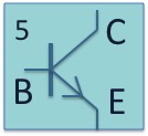
The very first bipolar junction transistors were fabricated from a bar of germanium with two closely spaced alloyed contacts. Germanium was used since it could easily be purified such that the minority carrier diffusion length was comparable to the distance between the two alloyed contacts. Starting with p-type germanium and using indium to form the alloyed junctions a discrete transistor was easily made. The germanium bar formed the base while the alloyed n-type regions formed the emitter and collector. Other implementations consisted of alloyed junctions on either side of a thin slice of germanium, with the emitter junction being smaller than the collector junction on the opposite side to ensure a high minority carrier collection efficiency on the collector side. |
5.8.2. First silicon IC technology |      |
The alloyed junction approach was soon abandoned and replaced by a double diffusion process, where the base and emitter region were formed by diffusion of dopants into the wafer. A low-doped collector region was epitaxially grown on the buried collector contact layer and isolation was obtained with a diffusion of opposite type. A similar process was also used to fabricate the first RTL (Resistor Transistor Logic) gates. It consists of the following steps: |
 |
| Figure 5.8.1. : | Diffusion isolated bipolar junction transistor with load resistor |
|
This process yields n-p-n bipolar transistors. Resistors were formed using the p-type base diffusion |
 |
| Figure 5.8.2. : | RTL inverter circuit and transfer characteristic |
A lateral pnp can be made with the same process as illustrated with Figure 5.8.3 |
 |
| Figure 5.8.3 : | Lateral pnp bipolar junction transistor |