7.3.1. The linear model


In this section, we present three different models for the MOSFET, the linear model, the quadratic model and the variable depletion layer model. The linear model correctly predicts the MOSFET behavior for small drain-source voltages, where the MOSFET acts as a variable resistor. The quadratic model includes the voltage variation along the channel between source and drain. This model is most commonly used despite the fact that the variation of the depletion layer charge is ignored. The variable depletion layer model is more complex, as it includes the variation of the depletion layer along the channel. |
7.3.1. The linear model |      |
The linear model describes the behavior of a MOSFET biased with a small drain-to-source voltage. As the name suggests, the linear model, describes the MOSFET acting as a linear device. More specifically, it can be modeled as a linear resistor whose resistance is modulated by the gate-to-source voltage. In this regime, the MOSFET can be used as a switch for analog and digital signals or as an analog multiplier. |
The general expression for the drain current equals the total charge in the inversion layer divided by the time the carriers need to flow from the source to the drain: |
 | (7.3.1) |
where Qinv is the inversion layer charge per unit area, W is the gate width, L is the gate length and tr is the transit time. If the velocity of the carriers is constant between source and drain, the transit time equals: |
 | (7.3.2) |
where the velocity, v, equals the product of the mobility and the electric field: |
 | (7.3.3) |
The constant velocity also implies a constant electric field so that the field equals the drain-source voltage divided by the gate length. This leads to the following expression for the drain current: |
 | (7.3.4) |
We now assume that the charge density in the inversion layer is constant between source and drain. We also assume that the basic assumption described in section 6.3.2 applies, namely that the charge density in the inversion layer equals minus the product of the capacitance per unit area and the gate-to-source voltage minus the threshold voltage: |
 | (7.3.5) |
The inversion layer charge is zero if the gate voltage is lower than the threshold voltage. Replacing the inversion layer charge density in the expression for the drain current yields the linear model: |
 | (7.3.6) |
Note that the capacitance in the above equations is the gate oxide capacitance per unit area. Also note that the drain current is zero if the gate-to-source voltage is less than the threshold voltage. The linear model is only valid if the drain-to-source voltage is much smaller than the gate-to-source voltage minus the threshold voltage. This insures that the velocity, the electric field and the inversion layer charge density is indeed constant between the source and the drain. |
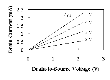
An example of the linear current-versus-voltage (I-V) characteristics of a MOSFET is shown in Figure 7.3.1. |
 |
| Figure 7.3.1 : | Linear I-V characteristics of a MOSFET with VT = 1 V. (μn = 300 cm2/V-s, W/L = 5 and tox = 20 nm).  |
The figure illustrates the behavior of the device in the linear regime: While there is no drain current if the gate voltage is less than the threshold voltage, the current increases with gate voltage once it is larger than the threshold voltage. The slope of the curves equals the conductance of the device, which increases linearly with the applied gate voltage. The figure therefore illustrates the use of a MOSFET as a voltage-controlled resistor. |
7.3.2. The quadratic model |      |
The quadratic model uses the same assumptions as the linear model. However, this model allows the inversion layer charge to vary between the source and the drain. |
The derivation is based on the fact that the current is continuous throughout the channel. The current is also related to the local channel voltage, >I>VC. |
We now consider a small section within the device with width dy>/I> and channel voltage VC + VS. The linear model as described by equation (7.3.6), still applies to such section, yielding: |
 | (7.3.7) |
where the drain-source voltage is replaced by the channel voltage. Both sides of the equation can be integrated from the source to the drain, so that y varies from 0 to the gate length, L, and the channel voltage VC varies from 0 to the drain-source voltage, VDS. |
 | (7.3.8) |
The drain current, ID, is constant so that integration results in: |
 | (7.3.9) |
The drain current first increases linearly with the applied drain-to-source voltage, but then reaches a maximum value. According to the above equation the current would even decrease and eventually become negative. The charge density at the drain end of the channel is zero at that maximum and changes sign as the drain current decreases. As explained in section 6.2, the charge in the inversion layer does go to zero and reverses its sign as holes are accumulated at the interface. However, these holes cannot contribute to the drain current since the reversed-biased p-n diode between the drain and the substrate blocks any flow of holes into the drain. Instead the current reaches its maximum value and maintains that value for higher drain-to-source voltages. A depletion layer located at the drain end of the gate accommodates the additional drain-to-source voltage. This behavior is referred to as drain current saturation. |
Drain current saturation therefore occurs when the drain-to-source voltage equals the gate-to-source voltage minus the threshold voltage. The value of the saturated drain current, ID,sat. is then given by the following equation: |
 | (7.3.10) |
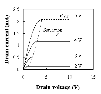
The quadratic model explains the typical current-voltage characteristics of a MOSFET, which are normally plotted for different gate-to-source voltages. An example is shown in Figure 7.3.2. The saturation occurs to the right of the dotted line which is given by ID = μ Cox W/L VDS2. |
 |
The drain current is still zero if the gate voltage is less than the threshold voltage. |
 | (7.3.11) |
For negative drain-source voltages, the transistor is in the quadratic regime and is described by equation (7.3.9). However, it is possible to forward bias the drain-bulk p-n junction. A complete circuit model should therefore also include the p-n diodes between the source, the drain and the substrate. |
We now use the quadratic model used to calculate some of the small signal parameters, namely the transconductance, gm and the output conductance, gd. |
The transconductance quantifies the drain current variation with a gate-source voltage variation while keeping the drain-source voltage constant, or: |
 | (7.3.12) |
The transconductance in the quadratic region is given by: |
 | (7.3.13) |
which is proportional to the drain-source voltage for VDS < VGS - VT. In saturation, the transconductance is constant and equals: |
 | (7.3.14) |
The output conductance quantifies the drain current variation with a drain-source voltage variation while keeping the gate-source voltage constant, or: |
 | (7.3.15) |
The output conductance in the quadratic region decreases with increasing drain-source voltage: |
 | (7.3.16) |
and becomes zero as the device is operated in the saturated region: |
 | (7.3.17) |
| Example 7.1 | Calculate the drain current of a silicon nMOSFET with VT = 1 V, W = 10 μm, L = 1 μm and tox = 20 nm. The device is biased with VGS = 3 V and VDS = 5 V. Use the quadratic model, a surface mobility of 300 cm2/V-s and set VBS = 0 V. Also calculate the transconductance at VGS = 3 V and VDS = 5 V and compare it to the output conductance at VGS = 3 V and VDS = 0 V. |
| Solution | The MOSFET is biased in saturation since VDS > VGS - VT. Therefore the drain current equals:
|
The measured drain current in saturation is not constant as predicted by the quadratic model. Instead it increases with drain-source voltage due to channel length modulation, drain induced barrier lowering or two-dimensional field distributions, as discussed in section 7.7. A simple empirical model, which considers these effects, is given by: |
 | (7.3.18) |
Where λ is a fitting parameter. |
7.3.3. The variable depletion layer model |      |
Next, we develop the variable depletion layer model, which includes the variation of the charge in the depletion layer between the source and drain. This variation is caused by the voltage variation along the channel. The inversion layer charge is still given by: |
 | (7.3.19) |
where we now include the implicit dependence of the threshold voltage on the charge in the depletion region, or: |
 | (7.3.20) |
The voltage VC is the difference between the voltage within the channel and the source voltage. We can now apply the linear model to a small section at a distance y from the source and with a thickness dy. The voltage at that point equals VC + VS while the voltage across that section equals dVC. This results in the following expression for the drain current, ID: |
 | (7.3.21) |
Both sides of the equation can be integrated from the source to the drain with y varying from 0 to the gate length, L, and the channel voltage, VC varying from 0 to the drain-source voltage, VDS. This results in: |
 | (7.3.22) |
Integration yields the following drain current: |
 | (7.3.23) |
The current-voltage characteristics as obtained with the above equation are shown in Figure 7.3.3, together with those obtained with the quadratic model. Again, it was assumed that the drain current saturates at its maximum value, since a positive inversion layer charge cannot exist in an n-type MOSFET. The drain voltage at which saturation occurs is given by: |
 | (7.3.24) |
 |
| Figure 7.3.3 : | Comparison of the quadratic model (upper curves) and the variable depletion layer model (lower curves)  |
The figure shows a clear difference between the two models: the quadratic model yields a larger drain current compared to the more accurate variable depletion layer charge model. The transconductance is still given by equation (7.3.13). This equation combined with the saturation voltage (equation (7.3.24)) yields: |
 | (7.3.25) |
This transconductance is almost linearly dependent on VGS, so that it can still be written in the form of equation (7.3.10) with a modified mobility μn*: |
 | (7.3.26) |
Where μn* equals: |
 | (7.3.27) |
The term under the square root depends on the ratio of the oxide capacitance to the depletion layer capacitance at the onset of inversion. Since this ratio is larger than one in most transistors, the modified mobility is 10% to 40% smaller than the actual mobility. This effective mobility can also be used with the quadratic model, yielding a simple but reasonably accurate model for the MOSFET. |
| Example 7.2 | Repeat example 7.1 using the variable depletion layer model. Use VFB = -0.807 V and Na = 1017 cm-3. |
| Solution | To find out whether the MOSFET is biased in saturation, one first calculates the saturation voltage, VD,sat:
|
Boulder, December 2004 |