
The SPICE model of a MOSFET includes a variety of parasitic circuit elements and some process related parameters in addition to the elements previously discussed in this chapter. The syntax of a MOSFET incorporates the parameters a circuit designer can control: |
MOSFET syntax |
M <name> <drain node> <gate node> <source node> <bulk/substrate node> |
+ |
+ [PD= |
+ [NRG= |
where L is the gate length, W the gate width, AD the drain area, AS the source area |
PD is the drain perimeter, PS is the source perimeter |
Example: |
M1 3 2 1 0 NMOS L=1u W=6u |
.MODEL NFET NMOS (LEVEL=2 L=1u W=1u VTO=-1.44 KP=8.64E-6 |
+ NSUB=1E17 TOX=20n) |
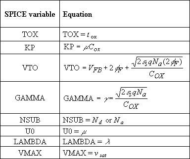
where M1 is one specific transistor in the circuit, while the transistor model "NFET" uses the built-in model NFET to specify the process and technology related parameters of the MOSFET. A list of selected SPICE parameters and their relation to the parameters discussed in this text is provided in the table below. |
 |
| Table 7.5.1: | SPICE parameters and corresponding equations |
In addition there are additional parameters, which can be specified to further enhance the accuracy of the model, such as: |
LD , lateral diffusion (length) |
RD, drain ohmic resistance |
RG, gate ohmic resistance |
IS, bulk p-n saturation current |
CBD, bulk-drain zero-bias p-n capacitance |
CGSO/CGDO, gate-source/drain overlap capacitance/channel width |
XJ, metallurgical junction depth |
WD, lateral diffusion (width) |
RS, source ohmic resistance |
RB, bulk ohmic resistance |
JS, bulk p-n saturation current/area |
CBS, bulk-source zero-bias p-n capacitance |
The gate-source/gate-drain overlap capacitance per channel width is obtained from: |
 |
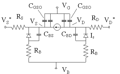
Where ΔL is the overlap between the gate and the source or drain region. The corresponding equivalent circuit is provided in Figure 7.5.1. |
 |
| Figure 7.5.1 : | Large signal model of a MOSFET |
The current source represents the drain current as described by either the quadratic model (equations (7.3.9) and (7.3.10)) or the variable depletion layer model (equations (7.3.23) and (7.3.24)). SPICE also allows the user to choose either model as well as other more detailed MOSFET models by selecting the model LEVEL. |
Boulder, December 2004 |