
The Metal-Oxide-Silicon Field-Effect-Transistor (MOSFET) is the primary driver in this industry, as it is the prevailing device in microprocessors and memory circuits. In addition, the MOSFET is increasingly used in areas as diverse as mainframe computers and power electronics. The MOSFET’s advantages over other types of devices are its mature fabrication technology, its successful scaling characteristics and the combination of complementary MOSFETs yielding CMOS circuits. The purpose of this text is to explore the internal behavior of semiconductor devices such as the MOSFET, so that one can understand the relation between the device geometry and material parameters on one hand, and the resulting electrical characteristics on the other hand. This text provides the link between the physics of semiconductors and the design of electronic circuits. The material covered in this text is therefore required to successfully design CMOS-based integrated circuits.
The fabrication process of silicon devices has evolved over the last 25 years into a mature, reproducible and reliable integrated circuit manufacturing technology. While the focus in this text is on individual devices, one must realize that the manufacturability of millions of such devices on a single substrate is a minimum requirement in today’s industry. Silicon has evolved as the material of choice for such devices, for a large part because of its stable oxide, silicon dioxide (SiO2), which is used as an insulator, as a surface passivation layer and as a superior gate dielectric. The scaling of MOSFETs started in the seventies. Since then, the initial 10 micron gatelength of the devices was gradually reduced by about a factor two every five years, while in 2000 MOSFETs with a 0.18 micron gatelength were manufactured on a large scale. This scaling is expected to continue well into the 21st century, as devices with a gatelength smaller than 20 nm have already been demonstrated. While the size reduction is a minimum condition when scaling MOSFETs, successful scaling also requires the reduction of all the other dimensions of the device so that the device indeed delivers superior performance. Devices with record gate lengths are typically not fully scaled, so that several years go by until the large-scale production of such device takes place.
This miniaturization trend is illustrated by the reduction of the minimum feature size and the resulting increase in number of transistors per die. Both are presented in Figure I.2.
 |
| Figure I.2: | Minimum feature size and number of transistors per die. |
The minimum feature size has steadily been reduced from about 10 mm in 1970 to 200 nm in 2000 and continues to further decrease with 45nm features currently going in production. The increase in number of device per die is only in part due to the reduction of the minimal feature size. As the technology has matured it has become possible to produce ever larger die with good yield. This trend goes hand in hand with the increase in wafer size, illustrated with Figure I.3.
 |
| Figure I.3: | Comparison of a 2 inch wafer to an 8 inch wafer. |
Shown is an 8 inch wafer as was primarily used around the year 2000 and compared to a 2 inch wafer as used in the 1970’s. The 8 inch wafer has a 16 times larger surface area, but also has less loss at the edges due to partial die especially as the die size increases. 8 inch wafers were recently replaced with 300 mm (about 12 inch) diameter wafers, almost doubling the wafer area.
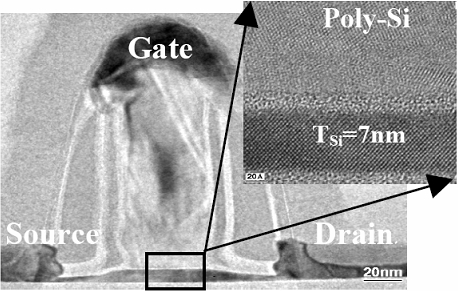
There has been much speculation as to how much longer this trend can be sustained, as there are economic, technological and physical limitations that are rapidly approaching. The gross national would have to increase, allowing the electronics market to further increase. Even larger production tools would have to be developed with better process control and accuracy. And even smaller devices have to be made, while the dimensions approach the atomic scale, resulting in undesired quantum effects. An example is shown in Figure I.4.
 |
| Figure I.4: | Cross-section of a MOSFET with 7nm thick channel and 2nm thick oxide. |
Shown is the cross section of a MOSFET with 45 nm gate length, 7 nm thick channel and 2 nm thick oxide. The inset is a transmission electron microscope (TEM) image, where on recognizes the arrangement of individual atoms in the channel, the random arrangement of atoms in oxide and the different orientations in the poly silicon gate.
Despite these looming limitations, the industry has not yet shown a sign that it is slowing down, and the device research and technological development is well underway to further sustain the current trend for the next 5-10 years.