2.2.1 Bravais lattices


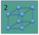
Solid materials are classified by the way the atoms are arranged within the solid. Materials in which atoms are placed at random are called amorphous. Materials in which atoms are placed in a highly ordered structure are called crystalline. Poly-crystalline materials are materials with a high degree of short-range order and no long-range order. These materials consist of small crystalline regions with random orientation called grains, separated by grain boundaries. Crystals naturally form as liquid material cools down, since the close proximity of atoms lowers their energy. However, since crystallization typically occurs in multiple locations simultaneously, one finds that the poly-crystalline structure is quite common except for materials such as glass which tend to be amorphous. Crystalline silicon dioxide does occur in the form of quartz but only if the temperature and pressure promote crystal formation. |
Crystalline semiconductors, in which atoms are placed in a highly ordered structure, are of primary interest in this text. Such materials are categorized by their crystal structure and the underlying lattice. While some crystals have a single atom placed at each lattice point, most crystals have a combination of atoms associated with each lattice point. This combination of atoms is also called the basis. |
The classification of lattices, the common semiconductor crystal structures and the growth of single-crystal semiconductors are discussed in the following sections. |
2.2.1 Bravais lattices |      |
The Bravais lattices are the distinct lattice types, which when repeated can fill the whole space. The lattice can therefore be generated by three unit vectors, |
| (2.2.1) |
The construction of the lattice points based on a set of unit vectors is illustrated by Figure 2.2.1. |
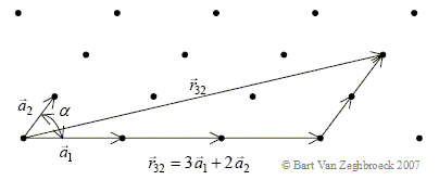 |
| Figure 2.2.1: | The construction of lattice points using unit vectors |
In two dimensions, there are five distinct Bravais lattices, while in three dimensions there are fourteen. The lattices in two dimensions are the square lattice, the rectangular lattice, the centered rectangular lattice, the hexagonal lattice and the oblique lattice as shown in Figure 2.2.2. It is customary to organize these lattices in groups, which have the same symmetry pproperties. An example is the rectangular and the centered rectangular lattice. As can be seen on the figure, all the lattice points of the rectangular lattice can be obtained by a combination of the lattice vectors |
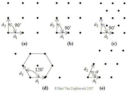 |
| Figure 2.2.2.: | The five Bravais lattices of two-dimensional crystals: (a) square, (b) rectangular, (c) centered rectangular, (d) hexagonal and (e) oblique |
The five Bravais lattices are mathematically described in Table 2.2.1. a1 and a2 are the magnitudes of the unit vectors and a is the angle between them. |
 |
| Table 2.2.1.: | Bravais lattices of two-dimensional crystals |
The same approach is used for lattices in three dimensions. The fourteen lattices of three-dimensional crystals are classified as shown in Table 2.2.2, where a1, a2 and a3 are the magnitudes of the unit vectors defining the traditional unit cell and α, β, and γ are the angles between these unit vectors. |
 |
| Table 2.2.2.: | Bravais lattices of three-dimensional crystals |
The cubic lattices are an important subset of these fourteen Bravais lattices since a large number of semiconductors have a cubic lattice. The three cubic Bravais lattices are the simple cubic (SC) lattice, the body-centered cubic (BCC) lattice and the face-centered cubic (FCC) lattice as shown in Figure 2.2.3. Since all unit vectors identifying the traditional unit cell have the same size, the crystal structure is completely defined by a single number, namely the lattice constant, a. |
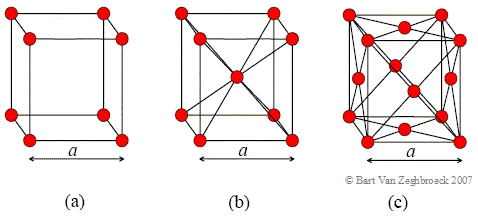 |
| Figure 2.2.3.: | a) The simple cubic (SC), b) the body-centered cubic (BCC), and c) the face centered cubic (FCC) lattice. |
2.2.2 Miller indices, crystal planes and directions |      |
Crystal planes of a crystal are characterized by their Miller indices. The Miller indices are defined as the smallest possible integers, which have the same ratios as the inverse of the intersections of a given plane with a set of axes defined by the unit vectors of that crystal. This definition is further illustrated with Figure 2.2.4. Orthogonal axes are used in this example, but the procedure is equally valid for any angle between the unit vectors. The intersections between the plane and the axis occur at p, q, and r. The corresponding Miller indices are therefore |
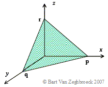 |
| Figure 2.2.4.: | Intersections of a plane and the x, y and z axes, as used to determine the Miller indices of the plane. |
2.2.3 Common semiconductor crystal structures |      |
The most common crystal structure among frequently used semiconductors is the diamond lattice, shown in Figure 2.2.5. Each atom in the diamond lattice has a covalent bond with four adjacent atoms, which together form a tetrahedron. This lattice can also be formed from two face-centered-cubic lattices, which are displaced along the body diagonal of the larger cube in Figure 2.2.5 by one quarter of that body diagonal. The diamond lattice therefore is a face-centered-cubic lattice with a basis containing two identical atoms. |
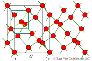 |
| Figure 2.2.5.: | The diamond lattice of silicon and germanium |
Compound semiconductors such as GaAs and InP have a crystal structure that is similar to that of diamond. However, the lattice contains two different types of atoms. Each atom still has four covalent bonds, but these are bonds to atoms of the other type. This structure is referred to as the zinc-blende lattice, named after zinc-blende crystal (ZnS) as shown in Figure 2.2.6. Both the diamond lattice and the zinc-blende lattice are cubic lattices. A third common crystal structure is the hexagonal structure also referred to as the wurzite crystal structure, which is the hexagonal form of zinc sulfide (ZnS). |
Many semiconductor materials can have more than one crystal structure. A large number of compound semiconductors including GaAs, GaN and ZnS can be either cubic or hexagonal. SiC can be cubic or one of several different hexagonal crystal structures. |
The cubic crystals are characterized by a single parameter, the lattice constant a, while the hexagonal structures are characterized in the hexagonal plane by a lattice constant a and by the distance between the hexagonal planes, c. |
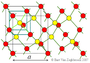 |
| Figure 2.2.6.: | The zinc-blende crystal structure of GaAs and InP |
Close packing of atoms results in a lower energy and therefore a preferred arrangement. Based on the table above, one finds that the FCC structure is preferred since the largest number of close neighbors results in the lowest energy of particles. However, the required number of chemical bonds must be satisfied at the same time. FCC crystals therefore typically occur when the strength of the chemical bonds is relatively weak such as for monovalent metals including copper, gold, and silver. Another example is opal, a gemstone, which consists of submicron silica spheres. Van der Waals forces dominate in this structure, while there is no further selection, as there are no chemical bonds. Opal is therefore a closed packed FCC structure. Group IV covalent semiconductors including silicon and germanium need to have four neighbors to obtain a fully filled outer shell by sharing their electrons in the outer shell with neighboring atoms. The diamond structure satisfies this requirement and is indeed the corresponding crystal structure. |
2.2.4 Growth of semiconductor crystals |      |
Like most crystals, semiconductor crystals can be obtained by cooling the molten semiconductor material. However, this procedure yields poly-crystalline material since crystals start growing in different locations with a different orientation. Instead, when growing single-crystalline silicon, one starts with a seed crystal and dips one end into the melt. By controlling the temperature difference between the seed crystal and the molten silicon, the seed crystal slowly grows. The result is a large single-crystal silicon boule. Such boules have a cylindrical shape, in part because the seed crystal is rotated during growth and in part because of the cylindrical shape of the crucible containing the melt. The boule is then cut into "wafers" with a diamond saw and further polished to yield the starting material for silicon device fabrication. |
truenano.com/PSD20 | Boulder, January 2026 |