3.2.1. Structure


3.2.1. Structure |      |
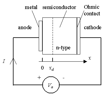
The structure of a metal-semiconductor junction is shown in Figure 3.2.1. It consists of a metal contacting a piece of semiconductor. An ideal Ohmic contact, a contact such that no potential exists between the metal and the semiconductor, is made to the other side of the semiconductor. The sign convention of the applied voltage and current is also shown on Figure 3.2.1. |
 |
| Figure 3.2.1 : | Structure and sign convention of a metal-semiconductor junction |
3.2.2. Flatband diagram and built-in potential |      |
The barrier between the metal and the semiconductor can be identified on an energy band diagram. To construct such diagram we first consider the energy band diagram of the metal and the semiconductor, and align them using the same vacuum level as shown in Figure 3.2.2 (a). As the metal and semiconductor are brought together, the Fermi energies of the metal and the semiconductor do not change right away. This yields the flatband diagram of Figure 3.2.2 (b). |
 |
| Figure 3.2.2 : | Energy band diagram of the metal and the semiconductor before (a) and after (b) contact is made. |
The barrier height, φB, is defined as the potential difference between the Fermi energy of the metal and the band edge where the majority carriers reside. From Figure 3.2.2 (b) one finds that for an n-type semiconductor the barrier height is obtained from: |
 | (3.2.1) |
Where ΦM is the work function of the metal and χ is the electron affinity. The work function of selected metals as measured in vacuum can be found in Table 3.2.1. For p-type material, the barrier height is given by the difference between the valence band edge and the Fermi energy in the metal: |
 | (3.2.2) |
A metal-semiconductor junction will therefore form a barrier for electrons and holes if the Fermi energy of the metal as drawn on the flatband diagram is somewhere between the conduction and valence band edge. |
In addition, we define the built-in potential, φI, as the difference between the Fermi energy of the metal and that of the semiconductor. |
 | (3.2.3) |
 | (3.2.4) |
The measured barrier height for selected metal-semiconductor junctions is listed in Table 3.2.1. These experimental barrier heights often differ from the ones calculated using (3.2.1) or (3.2.2). This is due to the detailed behavior of the metal-semiconductor interface. The ideal metal-semiconductor theory assumes that both materials are infinitely pure, that there is no interaction between the two materials and no unwanted interfacial layer. Chemical reactions between the metal and the semiconductor alter the barrier height as do interface states at the surface of the semiconductor and interfacial layers. Some general trends however can still be observed. As predicted by (3.2.1),the barrier height on n-type semiconductors increases for metals with a higher work function as can be verified for silicon. Gallium arsenide on the other hand is known to have a large density of surface states so that the barrier height becomes virtually independent of the metal. Furthermore, one finds that the barrier heights reported in the literature to vary widely due to different surface cleaning procedures. |
 |
| Table 3.2.1: | Workfunction in units of eV of selected metals and their measured barrier height on germanium, silicon and gallium arsenide. |
| Example 3.1 | Consider a chrome-silicon metal-semiconductor junction with Nd = 1017 cm-3. Calculate the barrier height and the built-in potential. Repeat for a p-type semiconductor with the same doping density. |
| Solution | The barrier height equals:
Note that this value differs from the one listed in Table 3.2.1 since the work function in vacuum was used. See the discussion in the text for more details. The built-in potential equals (using (3.2.3) and (2.6.12)):
The barrier height for the chrome/p-silicon junction equals:
And the built-in potential equals:
|
3.2.3. Thermal equilibrium |      |
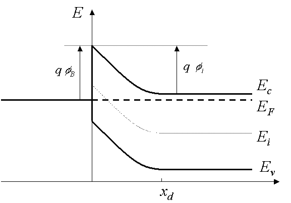
The flatband diagram, shown in Figure 3.2.2 (b), is not a thermal equilibrium diagram, since the Fermi energy in the metal differs from that in the semiconductor. Electrons in the n-type semiconductor can lower their energy by traversing the junction. As the electrons leave the semiconductor, a positive charge, due to the ionized donor atoms, stays behind. This charge creates a negative field and lowers the band edges of the semiconductor. Electrons flow into the metal until equilibrium is reached between the diffusion of electrons from the semiconductor into the metal and the drift of electrons caused by the field created by the ionized impurity atoms. This equilibrium is characterized by a constant Fermi energy throughout the structure. |
 |
| Figure 3.2.3 : | Energy band diagram of a metal-semiconductor contact in thermal equilibrium. |
It is of interest to note that in thermal equilibrium, i.e. with no external voltage applied, there is a region in the semiconductor close to the junction (0 ≤ x ≤ xd), which is depleted of mobile carriers. We call this the depletion region. The potential across the semiconductor equals the built-in potential, φi. |
3.2.4. Forward and reverse bias |      |
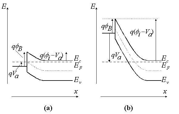
Operation of a metal-semiconductor junction under forward and reverse bias is illustrated with Figure 3.2.4. As a positive bias is applied to the metal (Figure 3.2.4 (a)), the Fermi energy of the metal is lowered with respect to the Fermi energy in the semiconductor. This results in a smaller potential drop across the semiconductor. The balance between diffusion and drift is disturbed and more electrons will diffuse towards the metal than the number drifting into the semiconductor. This leads to a positive current through the junction at a voltage comparable to the built-in potential. |
 |
| Figure 3.2.4 : | Energy band diagram of a metal-semiconductor junction under (a) forward and (b) reverse bias |
As a negative voltage is applied (Figure 3.2.4 (b)),the Fermi energy of the metal is raised with respect to the Fermi energy in the semiconductor. The potential across the semiconductor now increases, yielding a larger depletion region and a larger electric field at the interface. The barrier, which restricts the electrons to the metal, is unchanged so that that barrier, independent of the applied voltage, limits the flow of electrons. The metal-semiconductor junction with positive barrier height has therefore a pronounced rectifying behavior. A large current exists under forward bias, while almost no current exists under reverse bias. |
The potential across the semiconductor therefore equals the built-in potential, fi, minus the applied voltage, Va. |
 | (3.2.5) |
Boulder, 2022 |