

Metal-semiconductor contacts are an obvious component of any semiconductor device. At the same time, such contacts cannot be assumed to have a resistance as low as that of two connected metals. In particular, a large mismatch between the Fermi energy of the metal and semiconductor can result is a high-resistance rectifying contact. A proper choice of materials can provide a low resistance Ohmic contact. However for a lot of semiconductors there is no appropriate metal available. Instead one then creates a tunnel contact. Such contact consists of a thin barrier – obtained by heavily-doping the semiconductor – through which carriers can readily tunnel. Thin interfacial layers also affect contact formation. Most metal-semiconductor contacts are annealed or alloyed after the initial deposition of the metal in an effort to further improve the contact resistivity. This section describes each of these contacts as well as an analysis of the contact resistance between a metal and a thin semiconductor layer. |
3.5.1. Ohmic contacts |      |
A metal-semiconductor junction results in an Ohmic contact (i.e. a contact with voltage independent resistance) if the Schottky barrier height, φB, is zero or negative. In such case, the carriers are free to flow in or out of the semiconductor so that there is a minimal resistance across the contact. For an n-type semiconductor, this means that the workfunction of the metal must be close to or smaller than the electron affinity of the semiconductor. For a p-type semiconductor, it requires that the workfunction of the metal must be close to or larger than the sum of the electron affinity and the bandgap energy. Since the workfunction of most metals is less than 5 V and a typical electron affinity is about 4 V, it can be problematic to find a metal that provides an Ohmic contact to p-type semiconductors with a large bandgap such as GaN or SiC. |
3.5.2. Tunnel contacts |      |
An alternate and more practical contact is a tunnel contact. Such contacts do have a positive barrier at the metal-semiconductor interface, but also have a high enough doping in the semiconductor that there is only a thin barrier separating the metal from the semiconductor. If the width of the depletion region at the metal-semiconductor interface is very thin, on the order of 3 nm or less, carriers can readily tunnel across such barrier. The required doping density for such contact is 1019 cm-3 or higher. |
3.5.3. Annealed and alloyed contacts |      |
The fabrication of Ohmic contacts frequently includes a high temperature step so that the deposited metals can either alloy with the semiconductor or the high-temperature anneal reduces the unintentional barrier at the interface. |
In the case of silicon, one can simply deposit a metal such as aluminum and obtain a reasonable Ohmic contact. However, subsequent annealing at 475°C in a reducing ambient such as forming gas (20:1 N2/H2) will further improve the contact resistivity. The temperature is chosen below the eutectic temperature of the Si/Al eutectic composition. Annealing at higher temperature causes the formation of Si/Al alloys, which in turn causes pits in the silicon. This effect is also referred to as spiking and when penetrating through an underlying p-n junction these “spikes” dramatically affect the quality of the p-n junction as can be observed in the form of an enhanced leakage current or reduced breakdown voltage. The use of a reducing atmosphere avoids any further oxidation of the metal during annealing, while it can also reduce any interfacial oxide between the metal and semiconductor. Aluminum deposited onto low-doped silicon (< 1015 cm-3) tends to form Schottky barriers, so that it is advantageous to provided a more-highly doped contact region underneath the contact metal. The small barrier height can be overcome through thermionic emission, while the contact resistance is further improved by creating a tunnel barrier using degenerately doped contact layers. |
Contacts to compound semiconductors require some more attention. Selecting a material with the right workfunction might still not result in the expected Ohmic contact. This is caused by pinning of the Fermi energy at the interface due to the large number of surface states at the metal-semiconductor interface. This only leaves the tunnel contact as a viable low resistance contact. To further improve the tunnel contact one adds dopants such as germanium in the case of an n-type contact and zinc in the case of a p-type contact to the metal. An anneal at 400°C in a forming gas ambient for ten minutes causes the dopants to alloy with the semiconductor, thereby forming a thin high-doped region as desired for a tunnel contact. |
3.5.4. Contact resistance to a thin semiconductor layer |      |
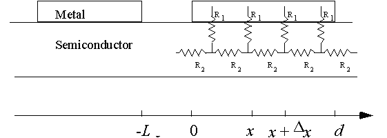
The contact between a metal and a thin semiconductor layer can be described with the resistive network shown in Figure 3.5.1. This equivalent circuit is obtained by slicing the structure into small sections with length Δx, so that the contact resistance, R1, and the semiconductor resistance, R2, are given by: |
 | (3.5.1) |
and |
 | (3.5.2) |
where ρc is the contact resistance of the metal-to-semiconductor interface per unit area with units of Ωcm2, Rs is the sheet resistance of the semiconductor layer with units of Ω/o Ohms per square), and W is the width of the contact. |
 |
| Figure 3.5.1 : | Distributed resistance model of a contact to a thin semiconductor layer. |
Using Kirchoff's laws one obtains the following relations between the voltage, V(x), across the M-S interface and the current, I(x), parallel to the interface at x and x + Δx. |
 | (3.5.3) |
 | (3.5.4) |
By letting Δx approach zero one finds the following differential equations for the current, I(x), and voltage, V(x): |
 | (3.5.5) |
 | (3.5.6) |
These equations can be combined into: |
 | (3.5.7) |
The parameter λ is the characteristic distance over which the current changes under the metal contact and is also referred to as the penetration length. The general solution for I(x) and V(x) are: |
 | (3.5.8) |
 | (3.5.9) |
Both are plotted in Figure 3.5.2: |
 |
| Figure 3.5.2: | Lateral current and voltage underneath a 5 µn;m long and 1 mm wide metal contact with a contact resistivity of 10-5 Ω-cm2 on a thin semiconductor layer with a sheet resistance of 100 Ω/o. |
The total resistance of the contact is: |
 | (3.5.10) |
In the limit for an infinitely long contact (or d >> λ) the contact resistance is given by: |
 | (3.5.11) |
A measurement of the resistance between a set of contacts with a variable distance L between the contacts (also referred to as a TLM structure) can therefore be fitted to the following straight line: |
 | (3.5.12) |
so that the resistance per square, Rs, can be obtained from the slope, while the contact resistivity, ρc, can be obtained from the intersection with the y-axis. The penetration depth, λ, can be obtained from the intersection with the x-axis. This is illustrated with Figure 3.5.3. |
 |
| Figure 3.5.3: | Resistance versus contact spacing, L, of a TLM structure. |
In the limit for a short contact (or d << λ), the contact resistance can be approximated by expanding the hyperbolic cotangent: |
 | (3.5.13) |
The total resistance of a short contact therefore equals the resistance between the contact metal and the semiconductor layer (i.e. the parallel connection of all the resistors, R1, in Figure 3.5.1), plus one third of the end-to-end resistance of the conducting layer underneath the contact metal (i.e. the series connection of all resistors, R2, in Figure 3.5.1). |
Boulder, 2022 |