4.5.1. General breakdown characteristics |   |
The maximum reverse bias voltage that can be applied to a p-n diode is limited by breakdown. Breakdown is characterized by the rapid increase of the current under reverse bias. The corresponding applied voltage is referred to as the breakdown voltage. |
The breakdown voltage is a key parameter of power devices. The breakdown of logic devices is equally important as one typically reduces the device dimensions without reducing the applied voltages, thereby increasing the internal electric field. |
Two mechanisms can cause breakdown, namely avalanche multiplication and quantum mechanical tunneling of carriers through the bandgap. Neither of the two breakdown mechanisms is destructive. However heating caused by the large breakdown current and high breakdown voltage causes the diode to be destroyed unless sufficient heat sinking is provided. |
Breakdown in silicon at room temperature can be predicted using the following empirical expression for the electric field at breakdown. |
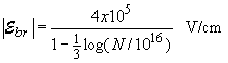 | (4.5.1) |
Assuming a one-sided abrupt p-n diode, the corresponding breakdown voltage can then be calculated, yielding: |
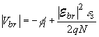 | (4.5.2) |
The resulting breakdown voltage is inversely proportional to the doping density if one ignores the weak doping dependence of the electric field at breakdown. The corresponding depletion layer width equals: |
 | (4.5.3) |
4.5.2. Edge effects | |
Few p-n diodes are truly planar and typically have higher electric fields at the edges. Since the diodes will break down in the regions where the breakdown field is reached first, one has to take into account the radius of curvature of the metallurgical junction at the edges. Most doping processes including diffusion and ion implantation yield a radius of curvature on the order of the junction depth, xj. The p-n diode interface can then be approximated as having a cylindrical shape along a straight edge and a spherical at a corner of a rectangular pattern. Both structures can be solved analytically as a function of the doping density, N, and the radius of curvature, xj. |
The resulting breakdown voltages and depletion layer widths are plotted below as a function of the doping density of an abrupt one-sided junction. |
 |
| Figure 4.5.1 : | Breakdown voltage and depletion layer width at breakdown versus doping density of an abrupt one-sided p-n diode. Shown are the voltage and width for a planar (top curves), cylindrical (middle curves) and spherical (bottom curves) junction with 1 mm radius of curvature. |
4.5.3. Avalanche breakdown | |
Avalanche breakdown is caused by impact ionization of electron-hole pairs. This process was described previously in section 2.8.When applying a high electric field, carriers gain kinetic energy and generate additional electron-hole pairs through impact ionization. The ionization rate is quantified by the ionization constants of electrons and holes, an and ap. These ionization constants are defined as the change of the carrier density with position divided by the carrier density or: |
 | (4.5.4) |
The ionization causes a generation of additional electrons and holes. Assuming that the ionization coefficients of electrons and holes are the same, the multiplication factor M, can be calculated from: |
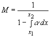 | (4.5.5) |
The integral is taken between x1 and x2, the region within the depletion layer where the electric field is assumed constant and large enough to cause impact ionization. Outside this range, the electric field is assumed to be too low to cause impact ionization. The equation for the multiplication factor reaches infinity if the integral equals one. This condition can be interpreted as follows: For each electron coming to the high field at point x1 one additional electron-hole pair is generated arriving at point x2. This hole drifts in the opposite direction and generates an additional electron-hole pair at the starting point x1. One initial electron therefore yields an infinite number of electrons arriving at x2, hence an infinite multiplication factor. |
The multiplication factor is commonly expressed as a function of the applied voltage and the breakdown voltage using the following empirical relation: |
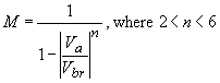 | (4.5.6) |
4.5.4. Zener breakdown | |
Quantum mechanical tunneling of carriers through the bandgap is the dominant breakdown mechanism for highly doped p-n junctions. The analysis is identical to that of tunneling in a metal-semiconductor junction (section 3.4.4.3) where the barrier height is replaced by the energy bandgap of the material. |
The tunneling probability equals: |
 | (4.5.7) |
where the electric field equals |
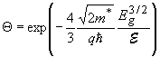
The tunneling current is obtained from the product of the carrier charge, velocity and carrier density. The velocity equals the Richardson velocity, the velocity with which on average the carriers approach the barrier while the carrier density equals the density of available electrons multiplied with the tunneling probability, yielding: |
 | (4.5.8) |
The tunneling current therefore depends exponentially on the bandgap energy to the 3/2 power. |
Boulder, November 2007 |
 = Eg/(qL).