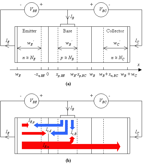

A bipolar junction transistor consists of two back-to-back p-n junctions, who share a thin common region with width, wB. Contacts are made to all three regions, the two outer regions called the emitter and collector and the middle region called the base. The structure of an npn bipolar transistor is shown in Figure 5.2.1 (a). The device is called “bipolar” since its operation involves both types of mobile carriers, electrons and holes. |
 |
| Figure 5.2.1.: | (a) Structure and sign convention of a npn bipolar junction transistor. (b) Electron and hole flow under forward active bias, VBE > 0 and VBC = 0. |
Since the device consists of two back-to-back diodes, there are depletion regions between the quasi-neutral regions. The width of the quasi neutral regions in the emitter, base and collector are indicated with the symbols wE', wB' and wC' and are calculated from |
 | (5.2.1) |
 | (5.2.2) |
 | (5.2.3) |
where the depletion region widths are given by: |
 | (5.2.4) |
 | (5.2.5) |
 | (5.2.6) |
 | (5.2.7) |
with |
 | (5.2.8) |
 | (5.2.9) |
The sign convention of the currents and voltage is indicated on Figure 5.2.1(a). The base and collector current are positive if a positive current goes into the base or collector contact. The emitter current is positive for a current coming out of the emitter contact. This also implies that the emitter current, IE, equals the sum of the base current, IB, and the collector current, IC: |
 | (5.2.10) |
The base-emitter voltage and the base-collector voltage are positive if a positive voltage is applied to the base contact relative to the emitter and collector respectively. |
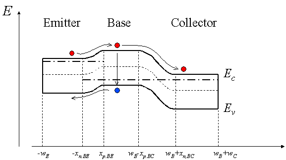
The operation of the device is illustrated with Figure 5.2.1 (b). We consider here only the forward active bias mode of operation, obtained by forward biasing the base-emitter junction and reverse biasing the base-collector junction. To simplify the discussion further, we also set VCE = 0. The corresponding energy band diagram is shown in Figure 5.2.2. Electrons diffuse from the emitter into the base and holes diffuse from the base into the emitter. This carrier diffusion is identical to that in a p-n junction. However, what is different is that the electrons can diffuse as minority carriers through the quasi-neutral base. Once the electrons arrive at the base-collector depletion region, they are swept through the depletion layer due to the electric field. These electrons contribute to the collector current. In addition, there are two more currents, the base recombination current, indicated on Figure 5.2.2 by the vertical arrow, and the base-emitter depletion layer recombination current, Ir,d, (not shown). |
 |
| Figure 5.2.2. : | Energy band diagram of a bipolar transistor biased in the forward active mode. |
The total emitter current is the sum of the electron diffusion current, IE,n, the hole diffusion current, IE,p and the base-emitter depletion layer recombination current, Ir,d. |
 | (5.2.11) |
The total collector current is the electron diffusion current, IE,n, minus the base recombination current, Ir,B. |
 | (5.2.12) |
The base current is the sum of the hole diffusion current, IE,p, the base recombination current, Ir,B and the base-emitter depletion layer recombination current, Ir,d. |
 | (5.2.13) |
The transport factor, a, is defined as the ratio of the collector and emitter current: |
 | (5.2.14) |
Using Kirchoff’s current law and the sign convention shown in Figure 5.2.1(a), we find that the base current equals the difference between the emitter and collector current. The current gain, b, is defined as the ratio of the collector and base current and equals: |
 | (5.2.15) |
This explains how a bipolar junction transistor can provide current amplification. If the collector current is almost equal to the emitter current, the transport factor, a, approaches one. The current gain, b, can therefore become much larger than one. |
To facilitate further analysis, we now rewrite the transport factor, a, as the product of the emitter efficiency, gE, the base transport factor, aT, and the depletion layer recombination factor, dr. |
 | (5.2.16) |
The emitter efficiency, gE, is defined as the ratio of the electron current in the emitter, IE,n, to the sum of the electron and hole current diffusing across the base-emitter junction, IE,n + IE,p. |
 | (5.2.17) |
The base transport factor, aT, equals the ratio of the current due to electrons injected in the collector, to the current due to electrons injected in the base. |
 | (5.2.18) |
Recombination in the depletion-region of the base-emitter junction further reduces the current gain, as it increases the emitter current without increasing the collector current. The depletion layer recombination factor, dr, equals the ratio of the current due to electron and hole diffusion across the base-emitter junction to the total emitter current: |
 | (5.2.19) |
| Example 5.1 | A bipolar transistor with an emitter current of 1 mA has an emitter efficiency of 0.99, a base transport factor of 0.995 and a depletion layer recombination factor of 0.998. Calculate the base current, the collector current, the transport factor and the current gain of the transistor. |
| Solution | The transport factor and current gain are:
and
The collector current then equals
And the base current is obtained from:
|