A large variety of bipolar junction transistor models have been developed. One distinguishes between small signal and large signal models. We will discuss here first the hybrid pi model, a small signal model, which lends itself well to small signal design and analysis. The next model is the charge control model, which is particularly well suited to analyze the large-signal transient behavior of a bipolar transistor. And we conclude with the derivation of the SPICE model parameters. |
5.6.1. Small signal model (hybrid pi model) |   |
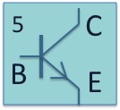
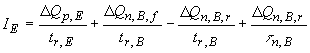
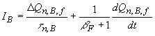
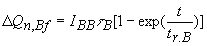
The hybrid pi model of a BJT is a small signal model, named after the “p”-like equivalent circuit for a bipolar junction transistor. The model is shown in Figure 5.6.1. It consists of an input impedance, rp, an output impedance r0, and a voltage controlled current source described by the transconductance, gm. In addition it contains the base-emitter capacitances, the junction capacitance, Cj,BE, and the diffusion capacitance, Cd,BE, and the base-collector junction capacitance, Cj,BC, also referred to as the Miller capacitance. |
 |
| Figure 5.6.1. : | Small signal model (hybrid pi model) of a bipolar junction transistor. |
The transconductance, gm, of a bipolar transistor is defined as the change in the collector current divided by the change of the base-emitter voltage. Using (5.4.6) one obtains: |
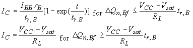
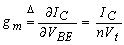 | (5.6.1) |
The base input resistance, rp, is defined as the change of the emitter-base voltage divided by the change of the base current. |
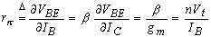 | (5.6.2) |
The output resistance, ro, is defined as: |
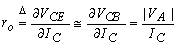 | (5.6.3) |
The base-emitter and base-collector junction capacitances are given by: |
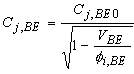 | (5.6.4) |
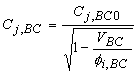 | (5.6.5) |
for the case where the base-emitter and base-collector junctions are abrupt. Since the base-emitter is strongly forward biased in the forward active mode of operation, one has to also include the diffusion capacitance of the base: |
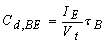 | (5.6.6) |
Based on the small signal model shown in Figure 5.6.1, we can now calculate the small signal current gain versus frequency, hfe, of a BJT biased in the forward active mode and connected in a common emitter configuration. The maximum current gain is calculated while shorting the output, resulting in: |
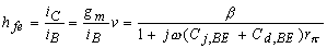 | (5.6.7) |
The unity gain frequency, fT, also called the transit frequency is obtained by setting the small signal current gain, hfe, equals to one, resulting in: |
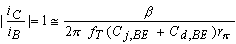 | (5.6.8) |
This transit frequency can be expressed as a function of the transit time, t: |
 | (5.6.9) |
Where the transit time, t, equals: |
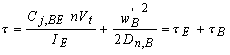 | (5.6.10) |
The circuit model therefore includes the charging time of the base-emitter capacitance, tE, as well as the base transit time, tB, but not the transit time of the carriers through the base-collector depletion region, tC. |
The collector transit time was presented in section 5.5.1. and described by equation (5.5.4), which is repeated here: |
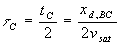 | (5.5.4) |
The total transit time then becomes: |
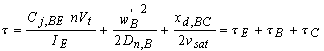 | (5.6.11) |
The corresponding transit frequency, fT, can still be calculated using (5.6.9). |
While the unity gain frequency, fT, is an important figure of merit of a bipolar transistor, another even more important figure of merit is the maximum oscillation frequency, fMAX. This figure of merit predicts the unity power gain frequency and as a result indicates the maximum frequency at which useful power gain can be expected from a device. The maximum oscillation frequency, fMAX, is linked to the transit frequency, fT, and is obtained from: |
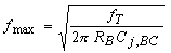 | (5.6.12) |
Where RB is the total base resistance and Cj,BC is the base-collector capacitance. The total base resistance consists of the series connection of metal-semiconductor contact resistance, the resistance between the base contact metal and the emitter and the intrinsic base resistance. Assuming a base contact, which is longer than the penetration depth this base resistance equals |
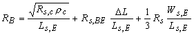 | (5.6.13) |
for a one-sided base contact, where Rs,c, Rs,BE and Rs are the sheet resistances under the base contact, between the base contact and the emitter and underneath the emitter respectively. Ls,E is the emitter stripe length of the emitter, Ws,E is the emitter stripe width of the emitter and DL is the alignment distance between the base contact and emitter. For a double-sided base contact, the total base resistance equals |
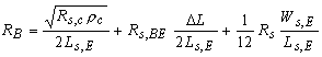 | (5.6.14) |
The base-collector capacitance equals: |
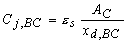 | (5.6.15) |
Where AC is the base-collector area. |
5.6.2. Large signal model (Charge control model) | |
The charge control model of a bipolar transistor is an extension of the charge control model of a p-n diode. Assuming the “short” diode model to be valid, one can express the device currents as a function of the charges in each region, divided by the corresponding transit or lifetime. In the general case one considers the forward bias charges as well as the reverse bias charges. This results in: |
 | (5.6.16) |
 | (5.6.17) |
 | (5.6.18) |
Under forward active mode of operation, this model can be simplified since the reverse mode components can be ignored. A transient model can be obtained by adding the rate of change of the charges over time. To further simplify the model, we also ignore the minority carrier charge, DQp,E, in the emitter. This results in the following equations: |
 | (5.6.19) |
 | (5.6.20) |
 | (5.6.21) |
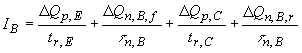
As an example we now apply this charge control model to the abrupt switching of a bipolar transistor. Consider the circuit shown in Figure 5.3.2.(a). As one applies a positive voltage to the base, the base-emitter junction will become forward biased so that the collector current will start to rise. The input is then connected to a negative supply voltage, VR. This reverses the base current and the base-emitter junction capacitance is discharged. After this transient, the transistor is eventually turned off and the collector current reduces back to zero. A full analysis would require solving the charge control model equations simultaneously, while adding the external circuit equations. Such approach requires numeric simulation tools. |
To simplify this analysis and provide insight, we now assume that the base current is constant before and after switching. This approximation is very good under forward bias since the base-emitter voltage is almost constant. Under reverse bias, the base current will vary as the base-emitter voltage varies, but conceivably one could design a circuit that does provide a constant reverse current. |
The turn-on of the BJT consists of an initial delay time, td,1, during which the base-emitter junction capacitance is charged. This delay is followed by the increase of the collector current, quantified by the rise time, trise. This rise time is obtained by applying the charge control equation for the base current, while applying a base current IBB with the voltage source VBB: |
 | (5.6.22) |
where: |
 | (5.6.23) |
This differential equation can be solved resulting in: |
 | (5.6.24) |
If the device does not reach saturation, the charge reaches its steady state value with a time constant tr,B, which equals the base transit time of the BJT. The corresponding collector current will be proportional to the excess minority carrier charge until the device reaches saturation or: |
 | (5.6.25) |
A larger base voltage, VBB, will therefore result in a larger charging current, IBB, which in turn decreases the rise time and causes the BJT to saturate more quickly. There also will be more excess minority carrier charge stored in the base region after the BJT is turned on. The rise time, trise, is then obtained by finding the time when the saturation current is reached or: |
 | (5.6.26) |
While switching back to the negative power supply, VR, the base current is reversed. As long as significant charge is still stored in the base region, the collector current will continue to exist. Only after this excess charge is removed, will the base-emitter junction capacitor be discharged and the BJT be turned off. The removal of the excess charge can take a significant delay time labeled as td,2 on the figure. Again we can calculate the time evolution of the excess charge and calculate the collector current from it. To first order the delay time, td,2, equals: |
 | (5.6.27) |
This delay time can be significantly larger than the rise time trise. Also note that a higher base turn-on current IBB results in a larger turn-off delay as more minority carrier charge is stored in the base. |
The actual fall time, tf, depends on the remaining storage charge at the onset of saturation as well as the charge stored by the base-emitter junction capacitance. |
 |
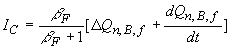
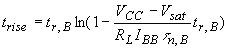
| Figure 5.6.2. : | Switching behavior of a BJT: a) bias circuit used to explain the switching behavior. b) Applied voltage and resulting collector current. |
5.6.3. SPICE model | |
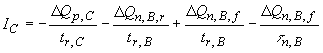
The SPICE model of a bipolar transistor includes a variety of parasitic circuit elements and some process related parameters in addition to the elements previously discussed in this chapter. The syntax of a bipolar transistor incorporates the parameters a circuit designer can change as shown below: |
BJT syntax |
Q |
+ [] |
.MODEL |
+ CJC= |
+ NF= |
BJT Parameters |
BF Forward active current gain |
BR Reverse active current gain |
IS Transport saturation current |
CJE Base-emitter zero-bias junction capacitance |
CJC Base-collector zero-bias Junction capacitance |
VJE Base-emitter built-in potential |
VJC Base-collector built-in potential |
VAF Forward mode Early voltage |
VAR Reverse mode Early voltage |
NF Forward mode ideality factor |
NR Reverse mode ideality factor |
Example: |
Q1 3 2 1 BJTNAME |
.MODEL BJTNAME NPN(BF=100 CJC=20pf CJE=20pf IS=1E-16) |
where Q1 is one specific transistor in the circuit, while the transistor model "BJTNAME" uses the built-in model NPN to specify the process and technology related parameters of the BJT. The built-in model PNP is used for p-n-p bipolar transistors. A list of SPICE parameters and their relation to the parameters discussed in this text is provided in the table below. |
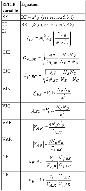 |
| Table 5.6.1. : | Selected SPICE parameters of a BJT. |
In addition, there are several parameters, which can be specified to further enhance the accuracy of the model, such as: |
RB base resistance |
RE emitter resistance |
RC collector resistance |
MJE base-emitter capacitance exponent |
MJC base-collector capacitance exponent |
EG energy gap for temperature effect on IS |
The exponents NJE and MJC are used to calculate the voltage dependence of the base-emitter and base-collector junction capacitances using: |
 | (5.6.28) |
 | (5.6.29) |
This exponent allows the choice between a uniformly doped junction (m = ˝), a linearly graded junction (m = 1/3) or an arbitrarily graded junction for which the exponent must be independently determined. |
The temperature dependence of the transport saturation current is calculated from the energy bandgap, since the primary temperature dependence is due to the temperature dependence of the intrinsic carrier density, which results in: |
 | (5.6.30) |
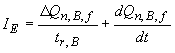
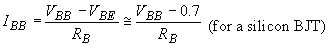
The corresponding equivalent circuit is provided in Figure 5.6.3. The output resistance, ro, was added to represent the Early effect, which is included in the BJT model by specifying VAF and VAR. |
 |
| Figure 5.6.3. : | Large signal model of a BJT including the junction capacitances. |