6.3.1. Flatband voltage calculation


6.3.1. Flatband voltage calculation |      |
If there is no charge present in the oxide or at the oxide-semiconductor interface, the flatband voltage simply equals the difference between the gate metal workfunction, FM, and the semiconductor workfunction, FS. |
 | (6.3.1) |
The workfunction is the voltage required to extract an electron from the Fermi energy to the vacuum level. This voltage is between three and five Volt for most metals. The actual value of the workfunction of a metal deposited onto silicon dioxide is not exactly the same as that of the metal in vacuum. Figure 6.3.1 provides experimental values for the workfunction of different metals, as obtained from a measurement on a MOS capacitor, as a function of the measured workfunction in vacuum. The same data is also listed in Table 6.3.1. |
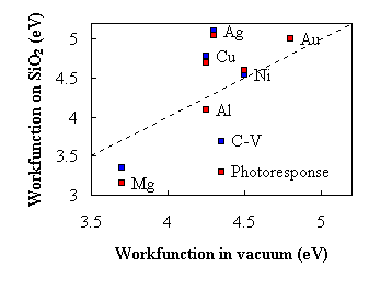 |
| Figure 6.3.1.: | Workfunction of Magnesium (Mg), Aluminum (Al), Copper (Cu), Silver (Ag), Nickel (Ni) and Gold (Au) obtained from I-V and C-V measurements on MOS structures as a function of the workfunction of those metals measured in vacuum. |
 |
| Table 6.3.1: | Workfunction of selected metals as measured in vacuum and as obtained from a C-V measurement on an MOS structure. |
The workfunction of a semiconductor, FS, requires some more thought since the Fermi energy varies with the doping type as well as with the doping concentration. This workfunction equals the sum of the electron affinity in the semiconductor, c, the difference between the conduction band energy and the intrinsic energy divided by the electronic charge in addition to the bulk potential. This is expressed by the following equation: |
 | (6.3.2) |
For MOS structures with a highly doped poly-silicon gate one must also calculate the workfunction of the gate based on the bulk potential of the poly-silicon. |
 | (6.3.3) |
Where Na,poly and Nd,poly are the acceptor and donor density of the p-type and n-type poly-silicon gate respectively. |
For a pMOS capacitor, which has an n-type substrate with doping density Nd, the workfunction difference equals: |
 | (6.3.4) |
The flatband voltage of real MOS structures is further affected by the presence of charge in the oxide or at the oxide-semiconductor interface. The flatband voltage still corresponds to the voltage, which, when applied to the gate electrode, yields a flat energy band in the semiconductor. Any charge in the oxide or at the interface affects the flatband voltage. For a charge, Qi, located at the interface between the oxide and the semiconductor, and a charge density, rox, distributed within the oxide, the flatband voltage is given by: |
 | (6.3.5) |
where the second term is the voltage across the oxide due to the charge at the oxide-semiconductor interface and the third term is due to the charge density in the oxide. |
The actual calculation of the flatband voltage is further complicated by the fact that charge can move within the oxide. The charge at the oxide-semiconductor interface due to surface states also depends on the position of the Fermi energy. |
Since any additional charge affects the flatband voltage and thereby the threshold voltage, great care has to be taken during fabrication to avoid the incorporation of charged ions as well as creation of surface states. |
| Example 6.1 | Calculate the flatband voltage of a silicon nMOS capacitor with a substrate doping Na = 1017 cm-3 and an aluminum gate (FM = 4.1 V). Assume there is no fixed charge in the oxide or at the oxide-silicon interface. |
| Solution | The flatband voltage equals the work function difference since there is no charge in the oxide or at the oxide-semiconductor interface.
|
6.3.2. Inversion layer charge |      |
The basis assumption as needed for the derivation of the MOSFET models is that the inversion layer charge is proportional with the applied voltage. In addition, the inversion layer charge is zero at and below the threshold voltage as described by: |
 | (6.3.6) |
The linear proportionality can be explained by the fact that a gate voltage variation causes a charge variation in the inversion layer. The proportionality constant between the charge and the applied voltage is therefore expected to be the gate oxide capacitance. This assumption also implies that the inversion layer charge is located exactly at the oxide-semiconductor interface. |
Because of the energy band gap of the semiconductor separating the electrons from the holes, the electrons can only exist if the p-type semiconductor is first depleted. The voltage at which the electron inversion-layer forms is referred to as the threshold voltage. |
To justify this assumption we now examine a comparison of a numeric solution with equation (6.3.6) as shown in Figure 6.3.2. |
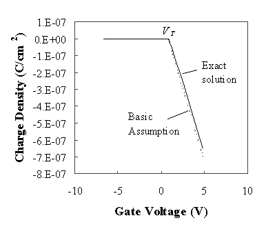 |
| Figure 6.3.2.: | Charge density due to electrons in the inversion layer of an MOS capacitor. Compared are the analytic solution (solid line) and equation (6.3.6) (dotted line) for Na = 1017 cm-3 and tox = 20 nm.  |
While there is a clear difference between the curves, the difference is small. We will therefore use our basic assumption when deriving the different MOSFET models since it dramatically simplifies the derivation, be it while losing some accuracy. |
6.3.3. Full depletion analysis |      |
We now derive the MOS parameters at threshold with the aid of Figure 6.3.3. To simplify the analysis we make the following assumptions: 1) we assume that we can use the full depletion approximation and 2) we assume that the inversion layer charge is zero below the threshold voltage. Beyond the threshold voltage we assume that the inversion layer charge changes linearly with the applied gate voltage. |
The derivation starts by examining the charge per unit area in the depletion layer, Qd. As can be seen in Figure 6.3.3 (a), this charge is given by: |
 | (6.3.7) |
Where xd is the depletion layer width and Na is the acceptor density in the substrate. Integration of the charge density then yields the electric field distribution shown in Figure 6.3.3 (b). The electric field in the semiconductor at the interface, |
 | (6.3.8) |
The electric field changes abruptly at the oxide-semiconductor interface due to the difference in the dielectric constant. At a silicon/SiO2 interface the field in the oxide is about three times larger since the dielectric constant of the oxide (eox = 3.9 e0) is about one third that of silicon (es = 11.9 e0). The electric field in the semiconductor changes linearly due to the constant doping density and is zero at the edge of the depletion region, based on the full depletion approximation. |
The potential shown in Figure 6.3.3 (c) is obtained by integrating the electric field. The potential at the surface, fs, equals: |
 | (6.3.9) |
 |
| Figure 6.3.3: | Electrostatic analysis of an MOS structure. Shown are (a) the charge density, (b) the electric field, (c) the potential and (d) the energy band diagram for an nMOS structure biased in depletion. |
The calculated field and potential is only valid in depletion. In accumulation, there is no depletion region and the full depletion approximation does not apply. In inversion, there is an additional charge in the inversion layer, Qinv. This charge increases gradually as the gate voltage is increased. However, this charge is only significant once the electron density at the surface exceeds the hole density in the substrate, Na. We therefore define the threshold voltage as the gate voltage for which the electron density at the surface equals Na. This corresponds to the situation where the total potential across the surface equals twice the bulk potential, fF. |
 | (6.3.10) |
The depletion layer in depletion is therefore restricted to this potential range: |
 | (6.3.11) |
For a surface potential larger than twice the bulk potential, the inversion layer charge increases exponentially with the surface potential. Consequently, an increased gate voltage yields an increased voltage across the oxide while the surface potential remains almost constant. We will therefore assume that the surface potential and the depletion layer width at threshold equal those in inversion. The corresponding expressions for the depletion layer charge at threshold, Qd,T, and the depletion layer width at threshold, xd,T, are: |
 | (6.3.12) |
 | (6.3.13) |
Beyond threshold, the total charge in the semiconductor has to balance the charge on the gate electrode, QM, or: |
 | (6.3.14) |
where we define the charge in the inversion layer as a quantity, which needs to determined but should be consistent with our basic assumption. This leads to the following expression for the gate voltage, VG: |
 | (6.3.15) |
In depletion, the inversion layer charge is zero so that the gate voltage becomes: |
 | (6.3.16) |
while in inversion this expression becomes: |
 | (6.3.17) |
the third term in (6.3.17) states our basic assumption, namely that any change in gate voltage beyond the threshold requires a change of the inversion layer charge. From the second equality in equation (6.3.17), we then obtain the threshold voltage or: |
 | (6.3.18) |
| Example 6.2 | Calculate the threshold voltage of a silicon nMOS capacitor with a substrate doping Na = 1017 cm-3, a 20 nm thick oxide (eox = 3.9 e0) and an aluminum gate (FM = 4.1 V). Assume there is no fixed charge in the oxide or at the oxide-silicon interface. |
| Solution | The threshold voltage equals:
|
6.3.4. MOS Capacitance |      |
Capacitance voltage measurements of MOS capacitors provide a wealth of information about the structure, which is of direct interest when one evaluates an MOS process. Since the MOS structure is simple to fabricate, the technique is widely used. |
To understand capacitance-voltage measurements one must first be familiar with the frequency dependence of the measurement. This frequency dependence occurs primarily in inversion since a certain time is needed to generate the minority carriers in the inversion layer. Thermal equilibrium is therefore not immediately obtained. |
The low frequency or quasi-static measurement maintains thermal equilibrium at all times. This capacitance is the ratio of the change in charge to the change in gate voltage, measured while the capacitor is in equilibrium. A typical measurement is performed with an electrometer, which measures the charge added per unit time as one slowly varies the applied gate voltage. |
The high frequency capacitance is obtained from a small-signal capacitance measurement at high frequency. The bias voltage on the gate is varied slowly to obtain the capacitance versus voltage. Under such conditions, one finds that the charge in the inversion layer does not change from the equilibrium value at the applied dc voltage. The high frequency capacitance therefore reflects only the charge variation in the depletion layer and the (rather small) movement of the inversion layer charge. |
In this section, we first derive the simple capacitance model, which is based on the full depletion approximation and our basic assumption. The comparison with the exact low frequency capacitance will reveal that the largest error occurs at the flatband voltage. We therefore derive the exact flatband capacitance using the linearized Poisson's equation. Then we discuss deep depletion as well as the non-ideal effects in MOS capacitors. |
The capacitance of an MOS capacitor is obtained using the same assumptions as those listed in section 6.3.3. The MOS structure is treated as a series connection of two capacitors: the capacitance of the oxide and the capacitance of the depletion layer. |
In accumulation, there is no depletion layer. The remaining capacitor is the oxide capacitance, so that the capacitance equals: |
 | (6.3.19) |
In depletion, the MOS capacitance is obtained from the series connection of the oxide capacitance and the capacitance of the depletion layer, or: |
 | (6.3.20) |
where xd is the variable depletion layer width which is calculated from: |
 | (6.3.21) |
In order to find the capacitance corresponding to a specific value of the gate voltage, we also need to use the relation between the potential across the depletion region and the gate voltage, given by: |
 | (6.3.16) |
In inversion, the capacitance becomes independent of the gate voltage. The low frequency capacitance equals the oxide capacitance since charge is added to and removed from the inversion layer. The high frequency capacitance is obtained from the series connection of the oxide capacitance and the capacitance of the depletion layer having its maximum width, xd,T. The capacitances are given by: |
 | (6.3.22) |
The capacitance of an MOS capacitor as calculated using the simple model is shown in Figure 6.3.4. The dotted lines represent the simple model while the solid line corresponds to the low frequency capacitance as obtained from the exact analysis. |
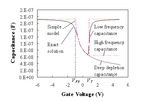 |
The simple model predicts that the flatband capacitance equals the oxide capacitance. However, the comparison with the exact solution of the low frequency capacitance as shown in Figure 6.3.4 reveals that the error can be substantial. The reason for this is that we have ignored any charge variation in the semiconductor. We will therefore now derive the exact flatband capacitance. |
To derive the actual flatband capacitance we first linearize Poisson's equation. Since the potential across the semiconductor at flatband is zero, we expect the potential to be small as we vary the gate voltage around the flatband voltage. Poisson's equation can then be simplified to: |
 | (6.3.23) |
Charge due to ionized donors or electrons were ignored, since neither are present in a p-type semiconductor around flatband. The linearization is obtained by replacing the exponential function by the first two terms of its Taylor series expansion. The solution to this equation is: |
 | (6.3.24) |
Where fs is the potential at the surface of the semiconductor and LD is the Debye length. The solution of the potential enables the derivation of the capacitance of the semiconductor under flatband conditions, or: |
 | (6.3.25) |
The flatband capacitance of the MOS structure at flatband is obtained by calculating the series connection of the oxide capacitance and the capacitance of the semiconductor, yielding: |
 | (6.3.26) |
| Example 6.3 | Calculate the oxide capacitance, the flatband capacitance and the high frequency capacitance in inversion of a silicon nMOS capacitor with a substrate doping Na = 1017 cm-3, a 20 nm thick oxide (eox = 3.9 e0) and an aluminum gate (FM = 4.1 V). |
| Solution | The oxide capacitance equals:
|
Deep depletion occurs in an MOS capacitor when measuring the high-frequency capacitance while sweeping the gate voltage "quickly". Quickly means that the gate voltage must be changed fast enough so that the structure is not in thermal equilibrium. One then observes that, when ramping the voltage from flatband to threshold and beyond, the inversion layer is not or only partially formed. This occurs since the generation of minority carriers cannot keep up with the amount needed to form the full inversion layer. The depletion layer therefore keeps increasing beyond its maximum thermal equilibrium value, xd,T resulting in a capacitance which further decreases with voltage. |
The time required to reach thermal equilibrium can be estimated by taking the ratio of the total charge in the inversion layer to the thermal generation rate of minority carriers. A complete analysis should include both the surface generation rate as well as generation in the depletion layer and the quasi-neutral region. A good approximation is obtained by considering only the generation rate in the depletion region and the quasi-neutral region. This yields the following equation: |
 | (6.3.27) |
where the generation in the depletion layer was assumed to be constant. For materials with a long diffusion length one can also ignore the generation in the depletion region. The rate of change required to observe deep depletion is then obtained from: |
 | (6.3.28) |
This equation predicts that deep depletion is less likely at higher ambient temperature, since the intrinsic carrier density ni increases exponentially with temperature. The intrinsic density also decreases exponentially with the energy bandgap. Therefore, MOS structures made with wide bandgap materials (for instance 6H-SiC for which Eg = 3 eV), have an extremely pronounced deep depletion effect. |
In silicon MOS capacitors, one finds that the occurrence of deep depletion can be linked to the minority carrier lifetime. Structures with a long (0.1 ms) lifetime require a few seconds to reach thermal equilibrium, which results in a pronounced deep depletion effect at room temperature. Structures with a short (1 ms) lifetime do not show this effect. |
Carrier generation due to light will increase the generation rate beyond the thermal generation rate and therefore reduces the time needed to reach equilibrium. Deep depletion measurements are therefore done in the dark. |
As an example, we present the measured low frequency (quasi-static) and high frequency capacitance-voltage curves of an MOS capacitor. The capacitance was measured in the presence of ambient light as well as in the dark as explained in the caption of Figure 6.3.5. |
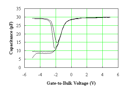 |
| Figure 6.3.5 : | Low frequency (quasi-static) and high frequency capacitance measurement of a pMOS capacitor. Shown are, from top to bottom, the low frequency capacitance measured in the presence of ambient light (top curve), the low frequency capacitance measured in the dark, the high frequency capacitance measured in the presence of ambient light and the high frequency capacitance measured in the dark (bottom curve). All curves were measured from left to right. The MOS parameters are Na - Nd = 4 x 1015 cm-3 and tox = 80 nm. The device area is 0.0007 cm2. |
Figure 6.3.5 illustrates some of the issues when measuring the capacitance of an MOS capacitance. First, one should measure the devices in the dark. The presence of light causes carrier generation in the semiconductor, which affects the measured capacitance. In addition, one must avoid the deep depletion effects such as the initial linearly varying capacitance of the high frequency capacitance measured in the dark on the above figure (bottom curve). The larger the carrier lifetime, the slower the voltage is to be changed to avoid deep depletion. |
The measured low frequency capacitance is compared to the theoretical value in Figure 6.3.6. The high frequency capacitance measured in the presence of light is also shown on the figure. The figure illustrates the agreement between experiment and theory. |
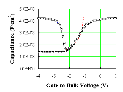 |
| Figure 6.3.6: | Comparison of the theoretical low frequency capacitance (solid line) and the experimental data (open squares) obtained in the dark. Fitting parameters are Na - Nd = 3.95 x 1015 cm-3 and tox = 80 nm. |
Non-ideal effects in MOS capacitors include fixed charge, mobile charge and charge in surface states. Performing a capacitance-voltage measurement can identify all three types of charge. |
Fixed charge in the oxide simply shifts the measured curve. A positive fixed charge at the oxide-semiconductor interface shifts the flatband voltage by an amount, which equals the charge divided by the oxide capacitance. The shift reduces linearly as one reduces the position of the charge relative to the gate electrode and becomes zero if the charge is located at the metal-oxide interface. A fixed charge is caused by ions, which are incorporated in the oxide during growth or deposition. |
The flatband voltage shift due to mobile charge is described by the same equation as that due to fixed charge. However, the measured curves differ since a positive gate voltage causes any negative mobile charge to move away from the gate electrode, while a negative voltage attracts the charge towards the gate. This causes the curve to shift towards the applied voltage. One can recognize mobile charge by the hysteresis in the high frequency capacitance curve when sweeping the gate voltage back and forth. Sodium ions incorporated in the oxide of silicon MOS capacitors are known to yield mobile charges. It is because of the high sensitivity of MOS structures to a variety of impurities that the industry carefully controls the purity of the water and the chemicals used. |
Charge due to electrons occupying surface states also yields a shift in flatband voltage. However as the applied voltage is varied, the Fermi energy at the oxide-semiconductor interface changes also and affects the occupancy of the surface states. The interface states cause the transition in the capacitance measurement to be less abrupt. The combination of the low frequency and high frequency capacitance allows a calculation of the surface state density. This method provides the surface state density over a limited (but highly relevant) range of energies within the bandgap. Measurements on n-type and p-type capacitors at different temperatures provide the surface state density throughout the bandgap. |