Throughout this text we have chosen to use nMOS capacitors are the preferred example. Several equations have only been provided for nMOS as those for pMOS are very similar. In this section we provide equations specifically for pMOS capacitors as well as a set of equations that could be applied to either type. |
6.7.1. pMOS equations |   |
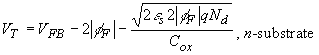
pMOS capacitors have an n-type substrate, a positive charge in the depletion layer and a positive charge in the inversion layer. Since the Fermi energy is a distance qfF/sub> above the midgap energy level, the workfunction difference is given by: |
 | (6.7.1) |
with |
 | (6.7.2) |
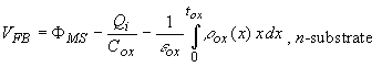
The expression for the depletion layer width is similar to that of nMOS capacitors, namely: |
 | (6.7.3) |
while the threshold is typically negative due to the positive charge in the depletion layer width. |
 | (6.7.4) |
Note that the relation between the flatband voltage and the workfunction difference still applies: |
 | (6.7.5) |
6.7.2. General equations | |
General equations, which are valid for n-MOS and p-MOS capacitors are provided below. The type is directly linked to the net doping density of the substrate, Na - Nd, which is positive for a p-type substrate (n-MOS capacitor) and negative for an n-type substrate (p-MOS capacitor). The workfunction difference is then given by: |
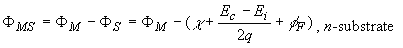 | (6.7.6) |
where the built-in potential is positive for p-type substrates and negative for n-type substrates and is given by: |
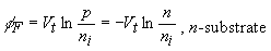 | (6.7.7) |
The depletion layer width at threshold is then: |
 | (6.7.8) |
and the threshold voltage is given by: |
 | (6.7.9) |
These equations are of interest when parameters of n-MOS as well as p-MOS capacitors are to be calculated. The equations eliminate the problem of the variable signs and possible mistakes and confusion, at the expense of the added complexity. |
In a MOSFET structure it is possible to apply a voltage, VC, to the channel relative to the voltage at the bulk contact to the substrate, VB. This affects the width of the depletion layer width at threshold: |
 | (6.7.10) |
as well as the threshold voltage itself: |
 | (6.7.11) |