A top view of the same MOSFET is shown in Figure 7.2.1, where the gate length, L, and gate width, W, are identified. Note that the gate length does not equal the physical dimension of the gate, but rather the distance between the source and drain regions underneath the gate. The overlap between the gate and the source/drain region is required to ensure that the inversion layer forms a continuous conducting path between the source and drain region. Typically this overlap is made as small as possible in order to minimize its parasitic capacitance. |
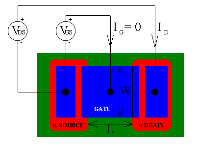 |
| Figure 7.2.1 : | Top view of an n-type Metal-Oxide-Semiconductor- Field-Effect-Transistor (MOSFET) |
The voltage applied to the gate controls the flow of electrons from the source to the drain. A positive voltage applied to the gate attracts electrons to the interface between the gate dielectric and the semiconductor. These electrons form a conducting channel called the inversion layer. No gate current is required to maintain the inversion layer at the interface since the gate oxide blocks any carrier flow. The net result is that the applied gate voltage controls the current between drain and source. |
The typical current versus voltage (I-V) characteristics of a MOSFET are shown in Figure 7.2.2. |
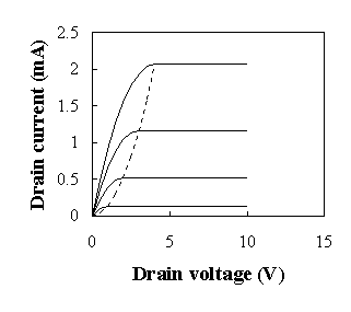 |
| Figure 7.2.2 : | I-V characteristics of an n-type MOSFET with VG = 5 V (top curve), 4 V, 3 V and 2 V (bottom curve) |
NOTE: We will primarily consider the n-type or n-channel MOSFET in this chapter. This type of MOSFET is fabricated on a p-type semiconductor substrate. The complementary MOSFET is the p-type or p-channel MOSFET. The p-type MOSFET contains p-type source and drain regions in an n-type substrate. The inversion layer is formed when holes are attracted to the interface by a negative gate voltage. While the holes still flow from source to drain, they result in a negative drain current. CMOS circuits require both n-type and p-type MOSFETs. |
Boulder, December 2004 |