The metal-semiconductor junction is the most studied unipolar junction, be not the only one that occurs in semiconductor devices. Two other unipolar junctions are the n-n+ homojunction and the n-n+ Heterojunction. |
The n-n+ homojunction frequently occurs in semiconductor devices are heavily doped regions are commonly added to reduce the overall resistance and improve the contact resistivity. Most textbooks ignore the effect of such junctions as the analysis is more difficult and the overall effect on the device is typically small. We present the electrostatic analysis of the n-n+ here in part for completeness but also to set the stage for the analysis of the n-n+ heterojunction. |
The n-n+ heterojunction frequently occurs in heterojunction devices. Such occurrence is not always deliberate, but their analysis is , albeit complex, need when optimizing a Heterojunction device design. |
In this section we present the electrostatic analysis of the n-n+ homojunction and heterojunction as well as the analysis of the n-n+ heterojunction current. |
3.8.1. The n-n+ homojunction |   |
When contacting semiconductor devices one very often includes highly doped semiconductor layers to lower the contact resistance between the semiconductor and the metal contact. This added layer causes a n-n+ junction within the device. Most often these junctions are ignored in the analysis of devices, in part because of the difficulty treating them correctly, in part because they can simply be ignored. The build-in voltage of a n-n+ junction is given by: |
 | (3.8.1) |
Which means that the built-in voltage is about 59.4 meV if the doping concentrations differ by a factor 10. It is because of this small built-in voltage that this junction is often ignored. However large variations in doping concentration do cause significant potential variations. |
The influence of the n-n+ junction must be evaluated in conjunction with its current voltage characteristics: if the n-n+ junction is in series with a p-n diode, the issue is whether or not the n-n+ junction affects the operation of the p-n junction in any way. At low current densities one can expect the p-n diode to dominate the current flow, whereas at high current densities the n-n+ junction could play a role if not designed properly. |
For the analysis of the n-n+ junction we start from a flat band energy band diagram connecting the two regions in absence of an electric field. One can visualize that electrons will flow from the n+ region and accumulate in the n-type region. However, since the carrier concentration must be continuous (this is only required in a homojunction), the carrier density in the n-type region is smaller that the doping concentration of the n+ region, and the n+ region is not completely depleted. The full depletion approximation is therefore not applicable. Instead one recognizes the situation to be similar to that of a metal-semiconductor junction: the n+ region is depleted but has a small voltage across the semiconductor as in a Schottky barrier with small applied voltage, whereas the n-type region is accumulated as in an Ohmic contact. A general solution of this structure requires the use of equation (3.3.2). |
An approximate solution can be obtained in the limit where the potential across both regions is smaller than the thermal voltage. The charge in the n-n+ structure region is then given by solving the linearized Poisson equation: |
 | (3.8.2) |
 | (3.8.3) |
where the n-n+ interface is located at x = 0, and LD,n and LD,n+ are the extrinsic Debye lengths in the material, given by: |
 | (3.8.4) |
 | (3.8.5) |
Applying Poisson's equation again one finds the potentials to be: |
 | (3.8.6) |
 | (3.8.7) |
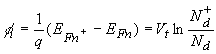
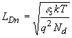
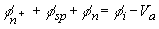
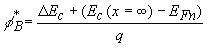
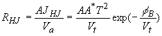
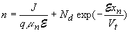
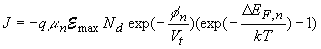
The solutions for the charge density, electric field, potential and energy band diagram are plotted in the Figure 3.8.1: |
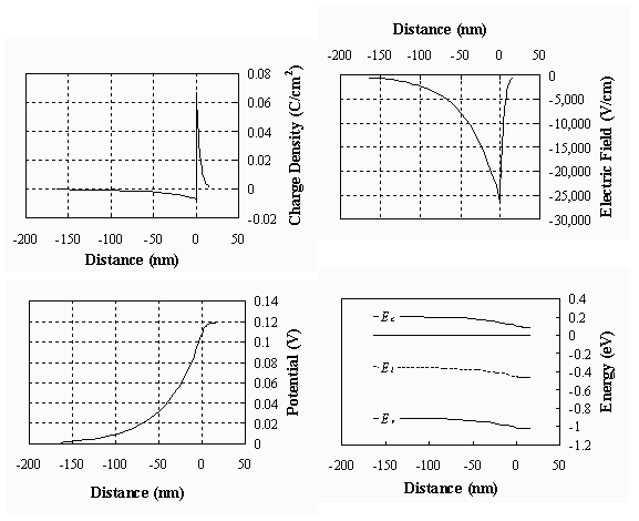 |
| Figure 3.8.1 : | Charge, electric field, potential and energy banddiagram in a silicon n-n+ structure with Nd = 1016 cm-3, Nd+ = 1017 cm-3 and Va = 0. |
3.8.2 The n-n+ heterojunction | |
Heterojunctions can be found in a wide range of heterojunction devices including laser diodes, high electron mobility transistors (HEMTs) and heterojunction bipolar transistors (HBTs). Of those, the HEMT naturally contains such heterojunction, while the other devices could contain an unintentional n-n+ heterojunction. |
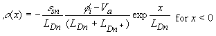
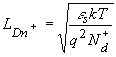
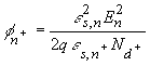
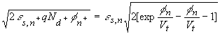
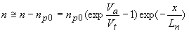
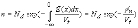
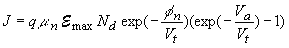
As a starting point of the analysis, consider a n-n+ heterojunction including a spacer layer with thickness d as shown in Figure 3.8.2. |
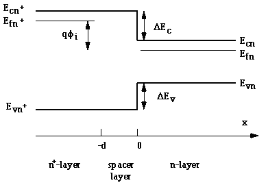 |
| Figure 3.8.2: | Flatband energy diagram of a n-n+ heterojunction including a spacer layer with thickness d. |
The built-in voltage for a n-n+ heterojunction with doping concentrations Nd and Nd+ is given by: |
 | (3.8.8) |
Where Nc,n and Nc,n+ are the effective densities of states of the low and high-doped region respectively. Unlike a homojunction, the heterojunction can have a built-in voltage, which is substantially larger than the thermal voltage. This justifies using the full depletion approximation for the depleted region. For the accumulated region one also has to consider the influence of quantization of energy levels as carriers are confined by the electric field and the hetero-interface. In the next two sections we analyze the energy band diagram of the n-n+ heterojunction with and without the inclusion of quantization and compare the two solutions. |
For the classic case where the material does not become degenerate at the interface one can use (3.3.22) to find the total charge in the accumulation layer: |
 | (3.8.9) |
while the potentials and the field can be solved for a given applied voltage using: |
 | (3.8.10) |
 | (3.8.11) |
 | (3.8.12) |
The subscript sp refers to the undoped spacer layer with thickness d, which is located between the two doped regions. These equations can be solved by starting with a certain value of fn, which enables the calculation of the electric field, the other potentials and the corresponding voltage, Va. |
The analysis of an n-n+ heterojunction including quantized levels is more complicated because the energy levels depend on the potential, which can only be calculated if the energy levels are known. A self-consistent calculation is therefore required to obtain a correct solution. An approximate method, which also clarifies the steps needed for a correct solution is described below. |
Starting from a certain density of electrons per unit area, Ns, which are present in the accumulation layer, one finds the field at the interface: |
 | (3.8.13) |
We assume that only the n = 1 energy level is populated with electrons. The minimal energy can be expressed as a function of the electric field: |
 | (3.8.14) |
The bandgap discontinuity DEc can then be related to the other potentials of the junction, yielding: |
 | (3.8.15) |
where the potentials, fn+ and fsp, in turn can be expressed as a function of |
 | (3.8.16) |
 | (3.8.17) |
These equations can be combined into one transcendental equation as a function of the electric field, |
 | (3.8.18) |
Once |
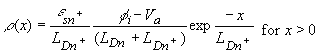
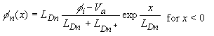
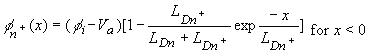
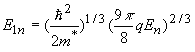
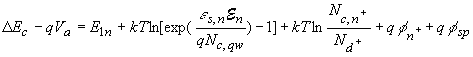
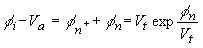
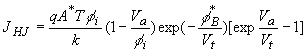
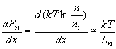
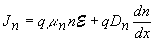
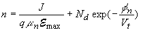
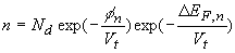
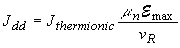
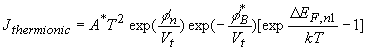
We now compare both approaches by presenting a numerical solution obtained by implementing the equations above for the case with as well as that without quantization. Keep in mind that neither is exact as it would require a self-consistent numerical analysis that includes the calculation of the potential based on the quantum mechanical distribution of the charge in each of the quantized levels. The energy band diagram and the sheet charge versus applied voltage are presented in Figure 3.8.3 and Figure 3.8.4 respectively. |
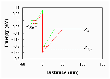 |
| Figure 3.8.3: | Energy banddiagram of a Al0.4Ga0.6As/GaAs n+-n heterostructure with Nd+ = 1017 cm-3, Nd = 1016 cm-3, d = 10 nm and Va = 0.15 V. Comparison of analysis without quantization (upper curve) to that with quantization (lower curve) |
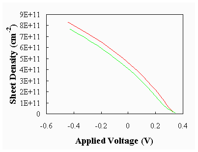 |
| Figure 3.8.4: | Electron density, Ns, in the accumulation region versus applied voltage, Va, with quantization (top curve) and without quantization (bottom curve). |
From the figures one finds that the analysis without quantization predicts a larger barrier to the left of the interface and a larger sheet charge for a given voltage. The actual solution is expected to be somewhere in between the two presented here, especially for the case where more than one quantized level exists and is occupied. |
3.8.3 Currents across a n+-n heterojunction | |
Current transport across a n+-n heterojunction is similar to that of a metal-semiconductor junction: Diffusion, thermionic emission as well as tunneling of carriers across the barrier can occur. However to identify the current components one must first identify the potentials fn+ and fn by solving the electrostatic problem. From the band diagram one finds that a barrier exists for electrons going from the n+ to the n-doped region as well as for electrons going in the opposite direction. |
The analysis in the first section discusses the thermionic emission and yields a closed form expression based on a set of specific assumptions. The derivation also illustrates how a more general expression could be obtained. The next section describes the current-voltage characteristics of carriers traversing a depletion region, while the last section discusses how both effects can be combined. |
The total current due to thermionic emission across the barrier is given by the difference of the current flowing from left to right and the current flowing from right to left. Rather than re-deriving the expression for thermionic emission, we will apply equation (3.4.6) to the n+-n heterojunction. One complication arises from the fact that the effective mass of the carriers is different on each side of the hetero-junction which would seem to indicate that the Richardson constant is different for carrier flow from left to right compared to the flow from right to left. A more detailed analysis reveals that the difference in effective mass causes a quantum mechanical reflection at the interface, causing carriers with the higher effective mass to be reflected back while carriers with the smaller effective mass are to first order unaffected. We therefore use equation (3.4.6) for flow in both directions while using the Richardson constant corresponding to the smaller of the two effective masses, yielding: |
 | (3.8.19) |
where the potentials are related to the applied voltage by: |
 | (3.8.20) |
and the built-in voltage is given by: |
 | (3.8.21) |
Combining these relations yields: |
 | (3.8.22) |
where the barrier height fB* is defined as: |
 | (3.8.23) |
Assuming full depletion in the n+ depletion region and using equation (3.8.9) for the accumulated region, the charge balance between the depletion and accumulation layer takes the following form: |
 | (3.8.24) |
Combining equations (3.2.20) with (3.2.16) yields a solution for fn+ and fn. |
For the special case where |
 | (3.8.25) |
The current (given by (3.2.18)) can then be expressed as a function of the applied voltage Va |
 | (3.8.26) |
Whereas this expression is similar to that of a metal-semiconductor barrier, it differs in that the temperature dependence is somewhat modified and the reverse bias current increases almost linearly with voltage. Under reverse bias, the junction can be characterized as a constant resistance, RHJ, which equals: |
 | (3.8.27) |
where A is the area of the junction. This shows that the resistance changes exponentially with the barrier height. Grading of the heterojunction is typically used to reduce the spike in the energy band diagram and with it the resistance across the interface. |
We typically assume the quasi-Fermi level to be constant throughout the depletion region. This assumption can be justified for a homojunction but is not necessarily correct for a heterojunction p-n diode. |
For a homojunction p-n diode we derived the following expression for the minority carrier density in the quasi-neutral region of a "long" diode |
 | (3.8.28) |
so that the maximum change in the quasi-Fermi level, which occurs at the edge of the depletion region, equals: |
 | (3.8.29) |
so that the change of the quasi-Fermi level can be ignored if the depletion region width is smaller than the diffusion length as is typically the case in silicon p-n diodes. |
For a hetero-junction p-n diode one can not assume that the quasi-Fermi level is continuous, especially when the minority carriers enter a narrow bandgap region in which the recombination rate is so high that the current is limited by the drift/diffusion current in the depletion region located in the wide bandgap semiconductor. |
The current density can be calculated from: |
 | (3.8.30) |
Assuming the field to be constant throughout the depletion region one finds for a constant current density the following expression for the carrier density at the interface: |
 | (3.8.31) |
While for zero current one finds, for an arbitrary field |
 | (3.8.32) |
Combining the two expressions we postulate the following expression for the carrier density: |
 | (3.8.33) |
The carrier density can also be expressed as a function of the total change in the quasi-Fermi level across the depletion region, DEfn; |
 | (3.8.34) |
which yields the following expressions for the current density due to drift/diffusion: |
 | (3.8.35) |
where is |
 | (3.8.36) |
which reduces for a M-S junction to: |
 | (3.8.37) |
so that thermionic emission dominates for vR << mn |
The calculation of the current through an n+-n junction due to thermionic emission and drift/diffusion becomes straightforward once one realizes that the total applied voltage equals the sum of the quasi-Fermi level variation, DEfn, across each region. For this analysis we therefore rewrite the current expressions as a function of DEfn, while applying the expression for the drift/diffusion current to the n+ material. |
 | (3.8.38) |
 | (3.8.39) |
 n:
n: