The transit time of electrons diffusing through the quasi-neutral region of the base was already introduced in section 5.3 and is given by: |
 | (5.5.1) |
This transit time corresponds to the average time the minority carriers need to traverse the quasi-neutral region in the base. Since the carriers move through this region by diffusion, it is the thermal energy, which causes the carrier motion. As a result, one occasionally finds that the base transit time decreases with increasing temperature. The junction temperature of BJTs in integrated circuits can therefore be significantly above room temperature without dramatically reducing the current gain, b, or the transit frequency, fT. The higher junction temperature also facilitates the heat transport from the collector - where most of the heat is generated - to the external heat sink. |
It is also of interest to note that the transit time is the same as the drift time of a majority carrier across a region of the same width if the applied voltage equals twice the thermal voltage. |
This simple transit time model must now be refined to include the drift through the base-collector depletion region. High injection, built-in fields and high current densities are known to further affect the total transit time through the device. |
5.5.1. Collector transit time through the base-collector depletion region |   |
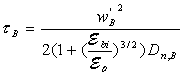
The transit time, tC, through the base-collector depletion region can be calculated by integrating the velocity across the depletion region, yielding: |
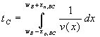 | (5.5.2) |
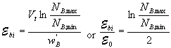
In principle, one could calculate the carrier velocity from the mobility and electric field in the depletion region. However, the full depletion approximation is no longer valid, since the zero field at the edge of the depletion region as described in section 4.3.3 causes an infinite transit time. The reality is that there is always a small field even at the edge of the depletion region and that a combination of drift and diffusion occurs. The calculation would therefore require an integration of the velocity as obtained through numeric simulation. A common approximation, which can be usually justified under high field conditions, is that the carrier velocity approaches the saturation velocity throughout the depletion region. The transit time for a single electron traversing the depletion region, then becomes: |
 | (5.5.3) |
The collector transit time, tC, in a bipolar transistor is the average delay of all carriers present in the depletion region relative to the point where they entered the base-collector depletion region. It is obtained from the integral of the conduction current including a frequency dependent phase across the depletion region divided by the depletion layer width. If the velocity is constant throughout the depletion region, the average delay is half of the transit time through the depletion region, or: |
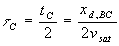 | (5.5.4) |
5.5.2. Base transit time in the presence of a built-in field | |
Varying the doping density throughout the base region can further reduce the base transit time. By decreasing the doping density from a maximum value, NB,MAX, on the emitter end, to a minimum value, NB,MIN, on the collector end, one obtains a built-in field in the base region. This built-in field increases the average velocity of the carriers and therefore shortens the base transit time. We now assume that the base doping decreases exponentially with position as illustrated with Figure 5.5.1a), or: |
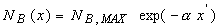 | (5.5.5) |
This results in a constant built-in electric field as indicated by Figure 5.5.1b). The base transit time is then obtained by solving the time-independent continuity equation including the built-in field. Such analysis results in a modified base transport time: |
 | (5.5.6) |
with |
 | (5.5.7) |
The built-in field in turn is calculated from the doping densities as: |
 | (5.5.8) |
For instance by grading the base doping from 1018 cm-3 to 1017 cm-3, |
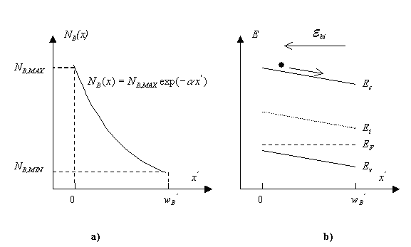 |
| Figure 5.5.1. : | a) Graded base doping with an exponential dependence, and b) Corresponding energy band diagram. |
5.5.3. Base transit time under high injection | |
High injection occurs when the minority carrier density in the base is equal or larger than the base doping density. Any further increase in the minority carrier density will then result in an almost equal increase in the majority carrier density, in order to maintain quasi-neutrality in the base. This then causes a gradient of the majority carriers equal to the gradient of the minority carrier density. This gradient causes a built-in electric field, which in turn reduces the transit time by a factor 2 resulting in: |
 | (5.5.9) |
This effect is referred to as the Webster effect. |
5.5.4. Kirk effect | |
The Kirk effect occurs at high current densities and causes a dramatic increase in the transit time of a bipolar transistor. The effect is due to the charge density associated with the current passing through the base-collector region. As this charge density exceeds the charge density in the depletion region the depletion region ceases to exist. Instead, there will be a build-up of majority carriers from the base in the base-collector depletion region. The dipole formed by the positively and negatively charged ionized donors and acceptors is pushed into the collector and replaced by positively charged ionized donors and a negatively charged electron accumulation layer, which is referred to as base push out. This effect occurs if the charge density associated with the current is larger than the ionized impurity density in the base-collector depletion region. Assuming full ionization, this translates into the following condition on the collector current density. |
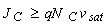 | (5.5.10) |
The effective width of the base layer then equals the width of the base and collector layer, which increases the transit time substantially. The increased transit time reduces the current gain and the transit frequency. |
Increasing the collector doping can easily eliminate the Kirk effect. However, this also increases the base-collector capacitance and decreases the collector-base breakdown voltage. As a results, the Kirk effect affects both RF and power devices. A proper trade-off between these factors is part of any device design and optimization. |
 bi/
bi/