Now that we have discussed the density of states and the distribution functions, we have all the necessary tools to calculate the carrier density in a semiconductor. |
2.6.1 General discussion |   |
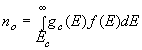
The density of electrons in a semiconductor is related to the density of available states and the probability that each of these states is occupied. The density of occupied states per unit volume and energy, n(E), ), is simply the product of the density of states in the conduction band, gc(E) and the Fermi-Dirac probability function, f(E), (also called the Fermi function): |
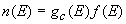 | (2.6.1) |
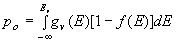
Since holes correspond to empty states in the valence band, the probability of having a hole equals the probability that a particular state is not filled, so that the hole density per unit energy, p(E), equals: |
 | (2.6.2) |
Where gv(E) is the density of states in the valence band. The density of carriers is then obtained by integrating the density of carriers per unit energy over all possible energies within a band. A general expression is derived as well as an approximate analytic solution, which is valid for non-degenerate semiconductors. In addition, we also present the Joyce-Dixon approximation, an approximate solution useful when describing degenerate semiconductors. |
The density of states in a semiconductor was obtained by solving the Schrödinger equation for the particles in the semiconductor. Rather than using the actual and very complex potential in the semiconductor, we use the simple particle-in-a box model, where one assumes that the particle is free to move within the material. |
For an electron which behaves as a free particle with effective mass, m*, the density of states was derived in section 2.4, yielding: |
 | (2.6.3) |
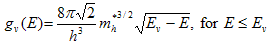
where Ec is the bottom of the conduction band below which the density of states is zero. The density of states for holes in the valence band is given by: |
 | (2.6.4) |
2.6.2. Calculation of the Fermi integral | |
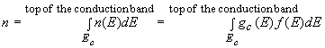
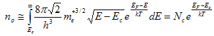
The carrier density in a semiconductor, is obtained by integrating the product of the density of states and the probability density function over all possible states. For electrons in the conduction band the integral is taken from the bottom of the conduction band, labeled, Ec, to the top of the conduction band: |
 | (2.6.5) |
Where gc(E) is the density of states in the conduction band and f(E) is the Fermi function. |
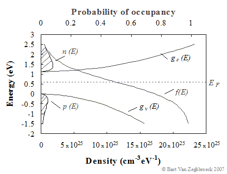
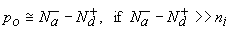
This general expression is illustrated with Figure 2.6.1 for a parabolic density of states function with Ec = 0. The figure shows the density of states function, gc(E), the Fermi function, f(E), as well as the product of both, which is the density of electrons per unit volume and per unit energy, n(E). The integral corresponds to the crosshatched area. |
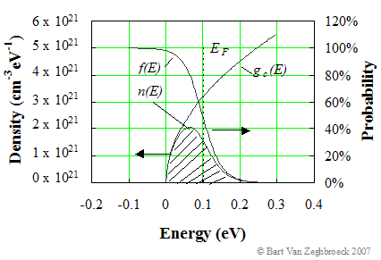 |
| Figure 2.6.1 : | The carrier density integral. Shown are the density of states, gc(E), the density per unit energy, n(E), and the probability of occupancy, f(E). The carrier density, no, equals the crosshatched area.  |
The actual location of the top of the conduction band does not need to be known as the Fermi function goes to zero at higher energies. The upper limit can therefore be replaced by infinity. We also relabeled the carrier density as no to indicate that the carrier density is the carrier density in thermal equilibrium. |
 | (2.6.6) |
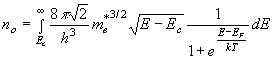 | (2.6.7) |
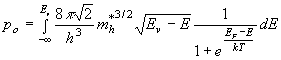
While this integral can not be solved analytically at non-zero temperatures, we can obtain either a numeric solution or an approximate analytical solution. Similarly for holes one obtains: |
 | (2.6.8) |
and |
 | (2.6.9) |
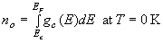
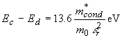
The calculation of the electron and hole density in a semiconductor is further illustrated by Figure 2.6.2. |
 |
| Figure 2.6.2 : | The density of states and carrier densities in the conduction and valence band. Shown are the electron and hole density per unit energy, n(E) and p(E), the density of states in the conduction and valence band, gc(E) and gv(E) and the probability of occupancy, f(E). The crosshatched area indicates the electron and hole densities. |
Indicated on the figure are the density of states in the conduction and valence band, the Fermi distribution function and the electron and hole densities per unit energy. The crosshatched areas indicate the thermal-equilibrium carrier densities. From the figure, one can easily see that the electron density will increase as the Fermi energy is increased. The hole density decreases with increasing Fermi energy. As the Fermi energy is decreased, the electron density decreases and the hole density increases. |
Equation (2.6.7) can be solved analytically at T = 0 K, since the Fermi function at T = 0 K equals one for all energies below the Fermi energy and 0 for all energies larger than the Fermi energy. Equation (2.6.7) can therefore be simplified to: |
 | (2.6.10) |
and integration yields: |
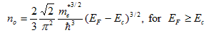 | (2.6.11) |
This expression can be used to approximate the carrier density in heavily degenerate semiconductors provided kT << (EF - Ec) > 0 |
Similarly, on obtains for holes: |
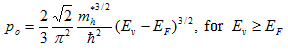 | (2.6.12) |
Non-degenerate semiconductors are defined as semiconductors for which the Fermi energy is at least 3kT away from either band edge. The reason we restrict ourselves to non-degenerate semiconductors is that this definition allows the Fermi function to be replaced with a simple exponential function, i.e. the Maxwell-Boltzmann distribution function. The carrier density integral can then be solved analytically yielding: |
 | (2.6.13) |
with |
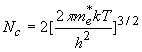 | (2.6.14) |
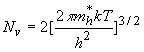
where Nc is the effective density of states in the conduction band. The Fermi energy, EF, is obtained from: |
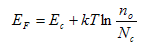 | (2.6.15) |
Similarly for holes, one can approximate the hole density integral as: |
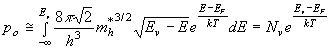 | (2.6.16) |
with |
 | (2.6.17) |
where Nv is the effective density of states in the valence band. The Fermi energy, EF, is obtained from: |
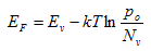 | (2.6.18) |
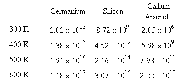
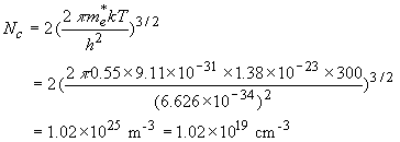
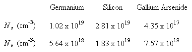
| Example 2.4 | Calculate the effective densities of states in the conduction and valence bands of germanium, silicon and gallium arsenide at 300 K. |
| Solution | The effective density of states in the conduction band of germanium equals:
where the effective mass for density of states was used (Appendix 3). Similarly one finds the effective densities for silicon and gallium arsenide and those of the valence band:
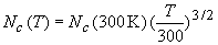
Note that the effective density of states is temperature dependent and can be obtain from:
where Nc(300 K) is the effective density of states at 300 K. |
A useful approximate expression applicable to degenerate semiconductors was obtained by Joyce and Dixon |
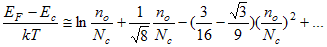 | (2.6.19) |
for electrons and by: |
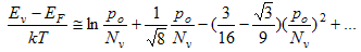 | (2.6.20) |
for holes. |
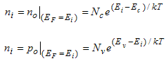
A comparison of the Joyce-Dixon approximation is presented in Figure 2.6.3. |
 |
| Figure 2.6.3 : | Carrier (electron) density versus Fermi energy, for Ec = 0 eV. Comparison of the Joyce Dixon approximation for degenerate semiconductors with equation (2.6.13) derived for non-degenerate semiconductors, equation (2.6.11) derived for T = 0 K and a numeric solution. |
Compared are the Joyce Dixon approximation with the solution derived for non-degenerate semiconductors, equation (2.6.13), the solution to the Fermi integral at zero Kelvin, equation (2.6.11), and a numeric solution. The Joyce Dixon approximation closely follows the numeric solution for all Fermi energies up to 0.1 eV beyond the conduction band edge, and carrier densities above 1020 cm-3. The zero temperature solution is a somewhat better fit at higher energies and carrier densities. |
2.6.3. Intrinsic semiconductors | |
Intrinsic semiconductors are semiconductors, which do not contain impurities. They do contain electrons as well as holes. The electron density equals the hole density since the thermal activation of an electron from the valence band to the conduction band yields a free electron in the conduction band as well as a free hole in the valence band. We will identify the intrinsic hole and electron density using the symbol ni, and refer to it as the intrinsic carrier density. |
Intrinsic semiconductors are usually non-degenerate, so that the expressions for the electron (2.6.12) and hole (2.6.14) densities in non-degenerate semiconductors apply. Labeling the Fermi energy of intrinsic material as Ei, we can then write two relations between the intrinsic carrier density and the intrinsic Fermi energy, namely: |
 | (2.6.21) |
It is possible to eliminate the intrinsic Fermi energy from both equations, simply by multiplying both equations and taking the square root. This provides an expression for the intrinsic carrier density as a function of the effective density of states in the conduction and valence band, and the bandgap energy Eg = Ec - Ev. |
 | (2.6.22) |
The temperature dependence of the intrinsic carrier density is dominated by the exponential dependence on the energy bandgap. In addition, one has to consider the temperature dependence of the effective densities of states and that of the energy bandgap. A plot of the intrinsic carrier density versus temperature is shown in Figure 2.6.4. |
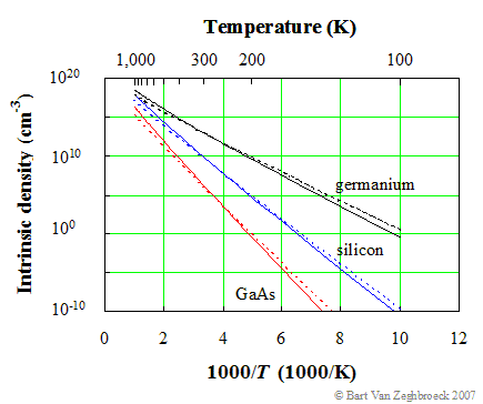 |
| Figure 2.6.4: | Intrinsic carrier density versus temperature in gallium arsenide (GaAs), silicon and germanium. Compared is the calculated density with (solid lines) and without (dotted lines) the temperature dependence of the energy bandgap. |
Compared is the calculated density using equation (2.6.22) with and without the temperature dependence of the energy bandgap described by equation (2.3.5). |
| Example 2.4b | Calculate the intrinsic carrier density in germanium, silicon and gallium arsenide at 300, 400, 500 and 600 K. |
| Solution | The intrinsic carrier density in silicon at 300 K equals:
Similarly one finds the intrinsic carrier density for germanium and gallium arsenide at different temperatures, yielding:
|
Note that the values at 300 K as calculated in example 2.4b are not identical to those listed in Appendix 3. This is due to an accumulation of assumptions in the derivation. The numbers in Appendix 3 are obtained from careful measurements and should therefore be used instead of those calculated in example 2.4b. |
Using the same approach as in section 2.6.3.1, one can prove that the product of the electron and hole density equals the square of the intrinsic carrier density for any non-degenerate semiconductor. By multiplying the expressions for the electron and hole densities in a non-degenerate semiconductor, as in equations (2.6.13) and (2.6.16), one obtains: |
 | (2.6.23) |
This property is referred to as the mass action law. It is a powerful relation, which enables to quickly find the hole density if the electron density is known or vice versa. This relation is only valid for non-degenerate semiconductors in thermal equilibrium. |
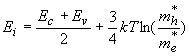
The above equations for the intrinsic electron and hole density can be solved for the intrinsic Fermi energy by taking the ratio of equations (2.6.21), yielding: |
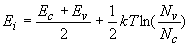 | (2.6.24) |
The intrinsic Fermi energy is typically close to the midgap energy, half way between the conduction and valence band edge. The intrinsic Fermi energy can also be expressed as a function of the effective masses of the electrons and holes in the semiconductor. For this we use equations (2.6.14) and (2.6.17) for the effective density of states in the conduction and valence band, yielding: |
 | (2.6.25) |
Dividing the expressions for the carrier densities (2.6.13) and (2.6.16), by those for the intrinsic density (2.6.21) allows to write the carrier densities as a function of the intrinsic density and the intrinsic Fermi energy, Ei, or: |
 | (2.6.26) |
and |
 | (2.6.27) |
We will use primarily these two equations to find the electron and hole density in a semiconductor in thermal equilibrium. The same relations can also be rewritten to obtain the Fermi energy from either carrier density, namely: |
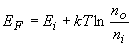 | (2.6.28) |
and |
 | (2.6.29) |
2.6.4. Doped semiconductors | |
Doped semiconductors are semiconductors, which contain impurities, foreign atoms incorporated into the crystal structure of the semiconductor. Either these impurities can be unintentional, due to lack of control during the growth of the semiconductor, or they can be added on purpose to provide free carriers in the semiconductor. |
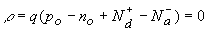
The generation of free carriers requires not only that impurities are present, but also that the impurities give off electrons to the conduction band in which case they are called donors. If they give off holes to the valence band, they are called acceptors (since they actually accept an electron from the filled valence band). The ionization of shallow donors and acceptors are illustrated by Figure 2.6.5. Indicated are the donor and acceptor energies, Ed and Ea. The donor energy level is filled prior to ionization. Ionization causes the donor to be emptied, yielding an electron in the conduction band and a positively charged donor ion. The acceptor energy is empty prior to ionization. Ionization of the acceptor corresponds to the empty acceptor level being filled by an electron from the filled valence band. This is equivalent to a hole given off by the acceptor atom to the valence band. |
 |
| Figure 2.6.5: | Ionization of a) a shallow donor and b) a shallow acceptor |
A semiconductor doped with impurities, which are ionized (meaning that the impurity atoms either have donated or accepted an electron), will therefore contain free carriers. Shallow impurities are impurities, which require little energy - typically around the thermal energy, kT, or less - to ionize. Deep impurities require energies much larger than the thermal energy to ionize so that only a fraction of the impurities present in the semiconductor contribute to free carriers. Deep impurities, which are more than five times the thermal energy away from either band edge, are very unlikely to ionize. Such impurities can be effective recombination centers, in which electrons and holes are captured and annihilate each other. Such deep impurities are also called traps. |
Ionized donors provide free electrons in a semiconductor, which is then called n-type, while ionized acceptors provide free holes in a semiconductor, which we refer to as being a p-type semiconductor. |
The ionization of the impurities is dependent on the thermal energy and the position of the impurity level within the energy band gap as described by the impurity distribution functions discussed in section 2.5.3. |
Shallow impurities readily ionize so that the free carrier density equals the impurity concentration. For shallow donors this implies that the electron density equals the donor concentration, or: |
 | (2.6.30) |
While for shallow acceptors the hole density equals the acceptor concentration, or: |
 | (2.6.31) |
If a semiconductor contains both shallow donors and shallow acceptors it is called compensated since equal amounts of donor and acceptor atoms compensate each other, yielding no free carriers. The presence of shallow donors and shallow acceptors in a semiconductor cause the electrons given off by the donor atoms to fall into the acceptor state, which ionizes the acceptor atoms without yielding a free electron or hole. The resulting carrier density in compensated material is approximately equal to the difference between the donor and acceptor concentration if the donor concentration is larger, yielding n-type material, or: |
 | (2.6.32) |
If the acceptor concentration is larger than the donor concentration, the hole density of the resulting p-type material equals the difference between the acceptor and donor concentration, or: |
 | (2.6.33) |
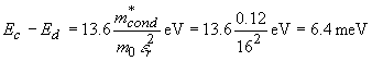
The energy required to remove an electron from a donor atom can be approximated using a hydrogen-like model. After all, the donor atom consists of a positively charged ion and an electron just like the proton and electron of the hydrogen atom. The difference however is that the average distance, r, between the electron and the donor ion is much larger since the electron occupies one of the outer orbitals. This is illustrated by Figure 2.6.6. |
 |
| Figure 2.6.6: | Trajectory of an electron bound to a donor ion within a semiconductor crystal. A 2-D square lattice is used for ease of illustration. |
For shallow donors, this distance, r, is much larger than the inter-atomic spacing of the semiconductor crystal. The ionization energy, Ed, can be estimated by modifying equation (1.2.10), which describes the electron energy in a hydrogen atom, yielding: |
 | (2.6.34) |
where m*condis the effective mass for conductivity calculations and εr is the relative dielectric constant of the semiconductor. The ionization energy is calculated as the difference between the energy of a free electron and that of an electron occupying the lowest energy level, E1. |
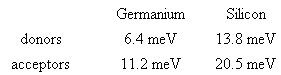
| Example 2.5 | Calculate the ionization energy for shallow donors and acceptors in germanium and silicon using the hydrogen-like model. |
| Solution | Using the effective mass for conductivity calculations (Appendix 3) one finds the ionization energy for shallow donors in germanium to be:
The calculated ionization energies for donors and acceptors in germanium and silicon are provided below.
Note that the actual ionization energies differ from these values and depend on the actual donor atom. |
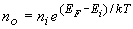
The calculation of the electron density starts by assuming that the semiconductor is neutral, so that there is no net charge in the material. This is a reasonable assumption since a net charge would result in an electric field. This electric field would move any mobile charge until it eliminates any charge imbalance. |
The charge density in a semiconductor depends on the free electron and hole density and on the ionized impurity densities. Ionized donors, which have given off an electron, are positively charged. Ionized acceptors, which have accepted an electron, are negatively charged. The total charge density is therefore given by: |
 | (2.6.35) |
The hole concentration in thermal equilibrium can be written as a function of the electron density by using the mass action law (2.6.23). This yields the following relation between the electron density and the ionized impurity densities: |
 | (2.6.36) |
Note that the use of the mass action law restricts the validity of this derivation to non-degenerate semiconductors as defined in section 2.6.2.2. Solving this quadratic equation yields a solution for the electron density, namely: |
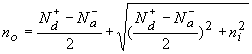 | (2.6.37) |
The same derivation can be repeated for holes, yielding: |
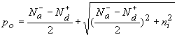 | (2.6.38) |
The above expressions provide the free carrier densities for compensated semiconductors assuming that all donors and acceptors are ionized. |
From the carrier densities, one then obtains the Fermi energies using equations (2.6.28) and (2.6.29) which are repeated below: |
| (2.6.28) |
or |
| (2.6.29) |
The calculated Fermi energies in n-type and p-type silicon as a function of doping density are shown in Figure 2.6.7 for different temperatures: |
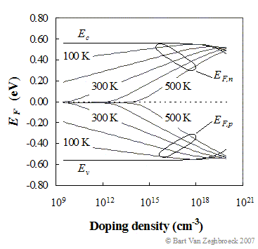 |
| Figure 2.6.7: | Fermi energy of n-type and p-type silicon, EF,n and EF,p, as a function of doping density at 100, 200, 300, 400 and 500 K. Shown are the conduction and valence band edges, Ec and Ev. The midgap energy is set to zero. |
Figure 2.6.7 illustrates how the Fermi energies vary with doping density. The Fermi energy varies linearly, when plotting the density on a logarithmic scale, up to a doping density of 1018 cm-3. This simple dependence requires that the semiconductor is neither intrinsic nor degenerate and that all the dopants are ionized. For compensated material, containing only shallow dopants, one uses the net doping density, |Nd - Na|. |
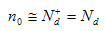
| Example 2.6a | A germanium wafer is doped with a shallow donor density of 3ni/2. Calculate the electron and hole density. |
| Solution | The electron density is obtained from equation (2.6.34) and the hole density is obtained using the mass action law:
|
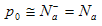
| Example 2.6b | A silicon wafer is doped with a shallow acceptor doping of 1016 cm-3. Calculate the electron and hole density. |
| Solution | Since the acceptor doping is much larger than the intrinsic density and much smaller than the effective density of states, the hole density equals: The electron density is then obtained using the mass action law The approach described in example 2.6a yields the same result.
|
A more general analysis takes also into account the fact that the ionization of the impurities is not 100%, but instead is given by the impurity distribution functions provided in section 2.5.3. |
The analysis again assumes that there is no net charge in the semiconductor (charge neutrality). This also means that the total density of positively charged particles (holes and ionized donors) must equals the total density of negatively charged particles (electrons and ionized acceptors) yielding: |
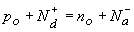 | (2.6.39) |
The electron and hole densities are then written as a function of the Fermi energy. For non-degenerate semiconductors one uses equations (2.6.12) and (2.6.15), while the ionized impurity densities equal the impurity density multiplied with the probability of occupancy for the acceptors and one minus the probability of occupancy for the donors. The Joyce-Dixon approximation, described in section (2.6.2.3) is used to calculate the degenerate carrier densities. |
A graphical solution to equation (2.6.39) above can be obtained by plotting both sides of the equation as a function of the Fermi energy as illustrated in Figure 2.6.8. |
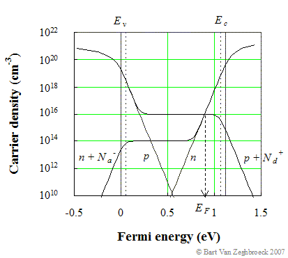 |
| Figure 2.6.8: | Graphical solution of the Fermi energy based on the general analysis. The value of the Fermi energy and the free carrier density is obtained at the intersection of the two curves, which represent the total positive and total negative charge in the semiconductor. Na equals 1016 cm-3 and Nd equals 1014 cm-3. |
Figure 2.6.8 shows the positive and negative charge densities as well as the electron and hole densities as a function of the Fermi energy. The dotted lines indicate the position of the acceptor and donor energies. The Fermi energy is obtained at the intersection of both curves as indicated by the arrow. |
This graphical solution is a very useful tool to explore the Fermi energy as a function of the doping densities, ionization energies and temperature. |
Operation of devices over a wide temperature range requires a detailed knowledge of the carrier density as a function of temperature. At intermediate temperatures the carrier density approximately equals the net doping, |Na - Nd|. Semiconductors, which satisfy this condition, are also called extrinsic semiconductors. The free carrier density increases at high temperatures for which the intrinsic density approaches the net doping density and decreases at low temperatures due to incomplete ionization of the dopants. The carrier density and Fermi energy are shown in Figure 2.6.9 for silicon doped with 1016 cm-3 donors and 1015 cm-3 acceptors: |
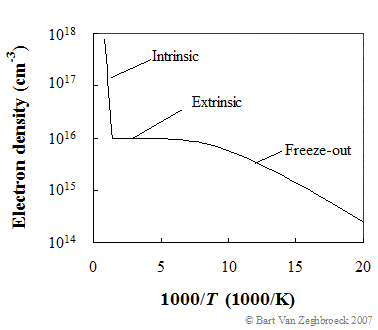 |
| Figure 2.6.9: | Electron density and Fermi energy as a function of temperature in silicon with Nd = 1016 cm-3, Na = 1014 cm-3 and Ec - Ed = Ea - Ev = 50 meV. The activation energy at 70 K equals 27.4 meV. |
At high temperatures, the carrier density equals the intrinsic carrier concentration, while at low temperatures the carrier density is dominated by the ionization of the donors. |
The temperature dependence is related to an activation energy by fitting the carrier density versus 1/T on a semi-logarithmic scale to a straight line of the form no(T) = C exp(-EA/kT), where C is a constant. At high temperatures this activation energy equals half the bandgap energy or EA = Eg/2. |
The temperature dependence at low temperatures is somewhat more complex as it depends on whether or not the material is compensated. Figure 2.6.9 was calculated for silicon containing both donors and acceptors. At 70 K the electron density is below the donor density but still larger than the acceptor density. Under such conditions the activation energy, EA, equals half of the ionization energy of the donors or (Ec - Ed)/2. At lower temperatures where the electron density is lower than the acceptor density, the activation energy equals the ionization energy or Ec - Ed. This behavior is explained by the fact that the Fermi energy in compensated material is fixed at the donor energy. The donors levels are always partially empty as electrons are removed from the donor atoms to fill the acceptor energy levels. If the acceptor density is smaller than the electron density � as is true for uncompensated material - the Fermi energy does change with temperature and the activation energy approaches half of the ionization energy. |
Lightly doped semiconductors suffer from freeze-out at relatively high temperature. Higher-doped semiconductors freeze-out at lower temperatures. Highly-doped semiconductors do not contain a single donor energy, but rather an impurity band which overlaps with the conduction or valence band. The overlap of the two bands results in free carriers even at zero Kelvin. Degenerately doping a semiconductor therefore eliminates freeze-out effects. |
The analysis of non-degenerate semiconductors can be further expanded to include carrier freeze-out in the presence of donors as well as acceptors. Equation (2.6.39) can be written as: |
 | (2.6.40) |
For n-type material (Nd > Na), this equation can be simplified to: |
 | (2.6.41) |
where the hole density, po, has been ignored and the acceptors are assumed to be fully ionized since the Fermi energy is expected to be above the energy of even the deepest acceptors. The density N* is given by: |
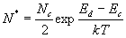 | (2.6.42) |
The solution to the quadratic equation is: |
 | (2.6.43) |
| Example 2.6c | 4H-SiC is doped with 2 x 1017 cm-3 nitrogen donor atoms (Ec � Ed = 90 meV). Use Nc = 4 x 1020 cm-3.
|
| Solution |
|
2.6.5. Non-equilibrium carrier densities | |
Up until now, we have only considered the thermal equilibrium carrier densities, no and po. However most devices of interest are not in thermal equilibrium. Keep in mind that a constant ambient constant temperature is not a sufficient condition for thermal equilibrium. In fact, applying a non-zero voltage to a device or illuminating it with light will cause a non-equilibrium condition, even if the temperature is constant. |
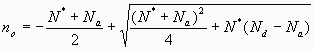
To describe a system that is not in thermal equilibrium we assume that each of the carrier distributions is still in equilibrium with itself. Such assumption is justified on the basis that electrons readily interact with each other and interact with holes only on a much longer time scale. As a result the electron density can still be calculated using the Fermi-Dirac distribution function, but with a different value for the Fermi energy. The total carrier density for a non-degenerate semiconductor is then described by: |
 | (2.6.44) |
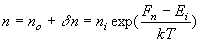
Where &delat;n is the excess electron density and Fn is the quasi-Fermi energy for the electrons. Similarly, the hole density can be expressed as: |
 | (2.6.45) |
Where &delat;p is the excess hole density and Fp is the quasi-Fermi energy for the holes. |
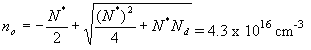
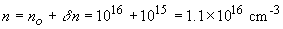
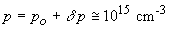
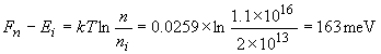
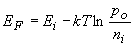
| Example 2.7 | A piece of germanium doped with 1016 cm-3 shallow donors is illuminated with light generating 1015 cm-3 excess electrons and holes. Calculate the quasi-Fermi energies relative to the intrinsic energy and compare it to the Fermi energy in the absence of illumination. |
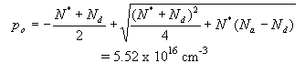
| Solution | The carrier densities when illuminating the semiconductor are:
and the quasi-Fermi energies are:
For comparison, the Fermi energy in the absence of light equals
which is very close to the quasi-Fermi energy of the majority carriers. |
| Boulder, 2022 |
 and is given by: