6.6.1. Introduction |   |
An exact analytic solution to Poisson’s equation can be obtained for the MOS capacitance as long as electron density at the surface is not degenerate. Poisson’s equation can then be solved yielding the electric field as a function of the potential in the semiconductor. A solution for the electric field and/or the potential as a function of position cannot be obtained analytically. This requires a numeric integration. Combining the electrical field and the surface potential yields the gate voltage, since the field in the semiconductor and that in the oxide are related by their respective dielectric constants. The same approach also yields a good approximation for the charge in the depletion layer, the inversion layer or the accumulation layer. The derivative of the charge with the applied voltage provides the capacitance of the MOS structure. The calculation of the low frequency or quasi-static capacitance is relative straight forward, while the calculation of the high-frequency capacitance requires an additional numeric integration. A detailed derivation of the items mentioned above including the deep depletion capacitance and the high-frequency capacitance are presented. We first examine and discuss the solution. |
6.6.2. Electric field versus surface potential | |
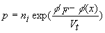
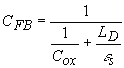
The solution for the electric field is presented in Figure 6.6.1. This figure was obtained for a substrate with an acceptor concentration, Na = 1017 cm-3, and an oxide thickness, tox = 20 nm. |
 |
| Figure 6.6.1 : | Electric field at the surface of the semiconductor as a function of the potential across the semiconductor. Shown is the absolute value of the electric field (solid line) and the field due to the inversion layer charge only (dashed line). The vertical dashed line indicates the threshold voltage. Na = 1017 cm-3, and tox = 20 nm. |
When applying a positive potential, for instance by applying a positive gate voltage, the surface of the silicon is initially depleted. This causes an electric field, which varies as the square root of the surface potential. At higher positive potential, the surface inverts resulting in a sharp rise of the electric field since the inversion layer charge increases exponentially with the surface potential. The vertical dotted line on the figure indicates the threshold voltage or the onset of strong inversion. The other dotted line represents the fraction of the surface field, which is due to the electrons in the inversion layer. It is calculated from the ratio of the inversion layer charge and the dielectric constant of the semiconductor. |
When applying a negative surface potential, the holes accumulate at the surface, yielding an exponential rise of the electric field with decreasing potential. |
6.6.3. Charge in the inversion layer | |
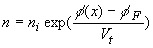
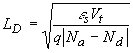
The total charge in the inversion layer is presented next. It is obtained by subtracting the charge in the depletion layer from the total charge for the same surface potential. The details can be found in section 6.6.5 . The gate voltage is obtained by adding the flatband voltage, the surface potential and the voltage across the oxide. The resulting charge density, plotted versus the gate voltage, is provided in Figure 6.6.2. This figure was calculated for an oxide thickness of 20 nm. The doping density is 1017 cm-3 as used in Figure 6.6.1. |
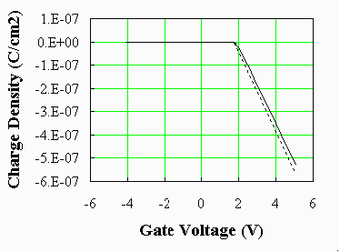 |
| Figure 6.6.2 : | Charge density due to electrons in the inversion layer of an MOS capacitor. Compared are the exact solution (solid line) and our basic assumption (dashed line). Na = 1017 cm-3, and tox = 20 nm. |
The dotted line on the figure represents the standard approximation for the inversion layer charge: it implies that the charge is simply proportional to the gate oxide capacitance and the gate voltage minus the threshold voltage. For voltages below the threshold voltage, there is no inversion layer and therefore no inversion layer charge. While not exact, the standard approximation is very good. |
6.6.4. Low frequency capacitance | |
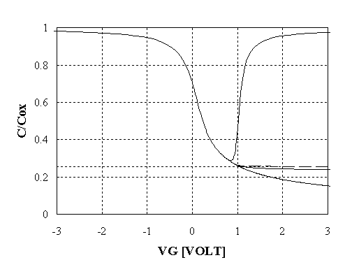
The low frequency or quasi-static capacitance is obtained by taking the derivative of the charge in the semiconductor with respect to the potential across the semiconductor. Since this derivative represents the change between two thermal equilibrium situations, this capacitance should be measured while maintaining equilibrium conditions at all times. The low frequency or quasi-static measurement is typically obtained by measuring the current with a sensitive electrometer while varying the applied gate voltage. |
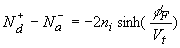
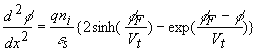
The expected behavior of such measurement is shown in Figure 6.6.3. The capacitance approaches the oxide capacitance except between the flatband voltage and the threshold voltage, as charge is then added at the edge of the depletion layer, rather than at the oxide-silicon interface. This results in the characteristic dip in the capacitance curve. |
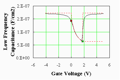 |
| Figure 6.6.3 : | Low frequency capacitance of an MOS capacitor. Shown is the exact solution for the low frequency capacitance (solid line) and the low and high frequency capacitance obtained with the simple model (dotted lines). The red square indicates the flatband voltage and capacitance, while the green square indicates the threshold voltage and capacitance. Na = 1017 cm-3, and tox = 20 nm. |
This figure was calculated using an oxide thickness of 20 nm and an acceptor concentration of 1017 cm-3. The dotted lines indicate the high- and low-frequency capacitance as obtained using the full depletion approximation. It is clear from the figure that the approximation is rather crude when it comes to describing the full behavior, but it is sufficient to extract the oxide thickness and substrate doping concentration from a capacitance-voltage measurement. |
6.6.5. Derivation of the exact solution | |
We now derive the exact solution of the MOS capacitor. Whereas most of the derivation is applicable for n-type and p-type substrates, the equations are written in a form, which is more convenient for p-type substrates. |
The total charge density, r, in the semiconductor is given by: |
 | (6.6.1) |
Under thermal equilibrium, the hole and electron densities, p and n, can be expressed as a function of the potential, f, and a reference potential, fF. |
 | (6.6.2) |
 | (6.6.3) |
Far away from the oxide-semiconductor interface, the charge density is zero and we define the potential, f, to be zero there also, so that |
 | (6.6.4) |
Poisson's equation then takes the following form: |
 | (6.6.5) |
Multiplying both sides of the equation with 2 df/dx and integrating while replacing -df/dx by the electric field |
 | (6.6.6) |
The constant K can be determined from the boundary condition at x = Ą where f = |
 | (6.6.7) |
The electric field has the same sign as the potential as indicated by the sign function. |
The relation between the field and the potential at the surface under thermal equilibrium is then: |
 | (6.6.8) |
The gate voltage equals the sum of the flatband voltage, the voltage across the oxide and the potential across the semiconductor: |
 | (6.6.9) |
The low frequency capacitance of the MOS structure per unit area can now be calculated from: |
 | (6.6.10) |
where Cox = |
 | (6.6.11) |
 | (6.6.12) |
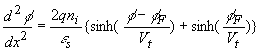
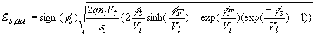
This result is often referred to as the low frequency capacitance of a MOS capacitor since we calculated the change in charge between two equilibrium situations. The result can be interpreted as a series connection of the oxide capacitance and the low frequency capacitance of the semiconductor Cs,LF. By starting from a series of values for fs, one can use the above equations to first calculate the electric field, the gate voltage and the capacitance. This enables to plot the low frequency capacitance as a function of the gate voltage as shown in Figure 6.6.4. |
 |
| Figure 6.6.4 : | Capacitance versus voltage for a MOS structure with Na = 1015 cm-3 and tox = 0.1 mm. The curves from top to bottom are: The low frequency capacitance, the approximate high frequency capacitance, the exact high frequency capacitance and the capacitance under deep depletion conditions. The dotted line indicates Cmin, the capacitance at the onset of strong inversion as calculated using the full depletion approximation. |
Under flatband conditions, where 0 = |fs| << Vt, the capacitance reduces to |
 | (6.6.13) |
where LD is the extrinsic Debye length in the semiconductor with doping |Na - Nd|: |
 | (6.6.14) |
If the gate voltage is changed faster than electrons can be generated at the oxide-semiconductor interface to obtain the equilibrium density, no inversion layer is generated. In this case the gate voltage will cause the depletion layer in the semiconductor to exceed the maximum depletion layer width as defined at the onset of strong inversion. A typical measurement starts from an equilibrium situation where no inversion layer is present and the gate voltage is swept rapidly while creating a depletion layer in the semiconductor. The capacitance is measured as the change in charge flowing into the structure for a given voltage change. For a p-type substrate, this situation can be modeled by eliminating the charge term due to electrons in Poisson's equation: |
 | (6.6.15) |
Using the same procedure as above the relation between surface field and surface potential can be found: |
 | (6.6.16) |
and the capacitance of the semiconductor becomes: |
 | (6.6.17) |
The corresponding gate voltage is: |
 | (6.6.18) |
Using a similar procedure as for the low frequency capacitance we can also plot the capacitance under deep depletion conditions. |
The high frequency capacitance of an MOS capacitor is measured by applying a small ac voltage in addition to the dc gate voltage. The capacitance is defined as the ratio of the out-of-phase component of the ac current divided by the amplitude of the ac voltage times the radial frequency. An approximate expression can be obtained by ignoring the change in charge in the inversion layer yielding the expression for the capacitance under deep depletion conditions. However since the gate voltage is changed slowly while measuring the capacitance versus voltage, the gate voltage is calculated from the surface potential including the charge in the inversion layer under thermal equilibrium. The capacitance is then given by: |
 | (6.6.19) |
with the electric field, |
This is the same expression as for the capacitance under deep depletion conditions. However, the corresponding gate voltage is different, namely: |
 | (6.6.20) |
where the electric field, |
The corresponding capacitance is also included in Figure 6.6.4 together with the expected minimum capacitance based on the full depletion approximation, corrected for the thermal voltage: |
 | (6.6.21) |
It should be noted that this is only an approximate solution. The redistribution of the inversion layer charge with applied gate voltage is ignored even though it does affect the depletion layer width and with it the capacitance. This approximation therefore introduces an error which was found to be less than 6% at the onset of strong inversion and which increases almost linearly with increasing surface potential. |
The exact expression for the high frequency capacitance used in Figure 6.6.4 is: |
 | (6.6.22) |
Where D for a p-type substrate is: |
 | (6.6.23) |
 | (6.6.24) |
The expression with D = 0 for all possible surface potentials equals the low frequency capacitance. The function F is related to the equilibrium electric field by: |
 | (6.6.25) |
and the normalized parameters U, Us and UF are defined as: |
 | (6.6.26) |
Where the gate voltage is still given by: |
 | (6.6.27) |
and the electric field, |
As illustrated with Figure 6.6.4, the high frequency capacitance at the onset of strong inversion (fs = 2fF) and beyond is found to be almost constant. Assuming fF >> Vt equation (6.6.19) becomes: |
 | (6.6.28) |
This result could also be obtained by calculating the depletion region width in the semiconductor assuming the maximum potential at the surface to be 2fF and using the full depletion approximation. |
The low frequency capacitance (equation (6.6.12)) at fs = 2fF, assuming fF >> Vt is then: |
 | (6.6.29) |
also yielding the following relation between both: |
 | (6.6.30) |
 , one obtains: