2.7.1. Carrier drift


Any motion of free carriers in a semiconductor leads to a current. This motion can be caused by an electric field due to an externally applied voltage, since the carriers are charged particles. We will refer to this transport mechanism as carrier drift. In addition, carriers also move from regions where the carrier density is high to regions where the carrier density is low. This carrier transport mechanism is due to the thermal energy and the associated random motion of the carriers. We will refer to this transport mechanism as carrier diffusion. The total current in a semiconductor equals the sum of the drift and the diffusion current. |
As one applies an electric field to a semiconductor, the electrostatic force causes the carriers to first accelerate and then reach a constant average velocity, v, due to collisions with impurities and lattice vibrations. The ratio of the velocity to the applied field is called the mobility. The velocity saturates at high electric fields reaching the saturation velocity. Additional scattering occurs when carriers flow at the surface of a semiconductor, resulting in a lower mobility due to surface or interface scattering mechanisms. |
Diffusion of carriers is obtained by creating a carrier density gradient. Such gradient can be obtained by varying the doping density in a semiconductor or by applying a thermal gradient. |
Both carrier transport mechanisms are related since the same particles and scattering mechanisms are involved. This leads to a relationship between the mobility and the diffusion constant called the Einstein relation. |
2.7.1. Carrier drift |      |
The motion of a carrier drifting in a semiconductor due to an applied electric field, |
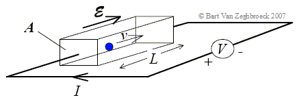 |
| Figure 2.7.1 : | Drift of a carrier due to an applied electric field. |
Assuming that all the carriers in the semiconductor move with the same average velocity, the current can be expressed as the total charge in the semiconductor divided by the time needed to travel from one electrode to the other, or: |
 | (2.7.1) |
where tr is the transit time of a particle, traveling with velocity, v, over the distance L. The current density, J, can then be rewritten as a function of the charge density, ρ : |
 | (2.7.2) |
If the carriers are negatively charged electrons, the current density equals: |
 | (2.7.2a) |
while for positively charged holes it is: |
 | (2.7.2b) |
Where n and p are the electron and hole density in the semiconductor. |
It should be noted that carriers do not follow a straight path along the electric field lines. Instead they bounce around in the semiconductor and constantly change direction and velocity due to scattering. This behavior occurs even when no electric field is applied and is due to the thermal energy of the carriers. Thermodynamics teaches us that electrons in a non-degenerate and non-relativistic electron gas have a thermal energy of kT/2 per particle per degree of freedom. A typical thermal velocity at room temperature is around 107 cm/s, which exceeds the typical drift velocity in semiconductors. The carrier motion in the semiconductor in the absence and in the presence of an electric field can therefore be visualized as in Figure 2.7.2. |
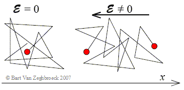 |
| Figure 2.7.2 : | Random motion of carriers in a semiconductor with and without an applied electric field. |
In the absence of an applied electric field, the carrier exhibits random motion and the carriers move quickly through the semiconductor and frequently change direction. When an electric field is applied, the random motion still occurs but in addition, there is on average a net motion along the direction of the field. Due to their different electronic charge, holes move on average in the direction of the applied field, while electrons move in the opposite direction. |
We now analyze the carrier motion considering only the average velocity, |
 | (2.7.3) |
The force consists of the difference between the electrostatic force and the scattering force due to the loss of momentum at the time of scattering. This scattering force equals the momentum divided by the average time between scattering events or collisions, τc, so that: |
 | (2.7.4) |
where a particle with charge q was assumed. |
Combining both relations yields an expression for the average particle velocity: |
 | (2.7.5) |
We now consider only the steady state situation in which the particle has already accelerated and has reached a constant average velocity. Under such conditions, the velocity is proportional to the applied electric field and we define the mobility as the velocity to field ratio: |
 | (2.7.6) |
The mobility of a particle in a semiconductor is therefore expected to be large if its mass is small and the time between scattering events is large. |
The drift current, described by (2.7.2), can then be rewritten as a function of the mobility, yielding: |
 | (2.7.7) |
For electrons and |
 | (2.7.8) |
For holes |
Throughout this derivation, we simply considered the mass, m, of the particle. However in order to incorporate the effect of the periodic potential of the atoms in the semiconductor we must use the effective mass, m*, rather than the free particle mass, m0, so that: |
 | (2.7.9) |
| Example 2.8 | Electrons in undoped gallium arsenide have a mobility of 8,800 cm2/V-s. Calculate the average time between collisions. Calculate the distance traveled between two collisions (also called the mean free path). Use an average velocity of 107 cm/s. |
| Solution | The collision time, τc, is obtained from:
where the mobility was first converted in MKS units. The mean free path, l, equals:
|
Impurities are foreign atoms in the semiconductor. They are efficient scattering centers especially when charged. Ionized donors and acceptors in a semiconductor are a common example of such impurities. The amount of scattering due to electrostatic forces between the carrier and the ionized impurity depends on the interaction time and the number of impurities. Larger impurity concentrations result in a lower mobility. The dependence on the interaction time helps to explain the temperature dependence. The interaction time is directly linked to the relative velocity of the carrier and the impurity, which is related to the thermal velocity of the carriers. The thermal velocity increases with the ambient temperature so that the interaction time decreases. Thereby, the amount of scattering decreases, resulting in a mobility increase with temperature. To first order, the mobility due to impurity scattering is proportional to T 3/2/NI, where NI is the density of charged impurities. |
Scattering by lattice waves includes the absorption or emission of either acoustical or optical phonons. These phonons represent quanta of mechanical waves that travel through the semiconductor crystal. Since the density of phonons in a solid increases with temperature, the scattering time due to this mechanism will decrease with temperature as will the mobility. Theoretical calculations reveal that the mobility in non-polar semiconductors, such as silicon and germanium, is dominated by acoustic phonon interaction. The resulting mobility is expected to be proportional to T -3/2, while the mobility due to optical phonon scattering only is expected to be proportional to T -1/2. Experimental values of the temperature dependence of the mobility in germanium, silicon and gallium arsenide are provided in Table 2.7.1[Ref. 3.1 pp28-30]. |
 |
| Table 2.7.1 : | Temperature dependence of the mobility in germanium, silicon and gallium arsenide due to phonon scattering |
The surface and interface mobility of carriers is affected by the nature of the adjacent layer or surface. Even if the carrier does not transfer into the adjacent region, its wavefunction does extend over 1 to 10 nanometer, so that there is a non-zero probability that the particle is in the adjacent region. The net mobility is then a combination of the mobility in both layers. For carriers in the inversion layer of a MOSFET, one finds that the mobility can be up to three times lower than the bulk value as further discussed in section 7.6.5. This is due to the distinctly lower mobility of electrons in the amorphous silicon oxide. The presence of charged surface states further reduces the mobility just as ionized impurities would. |
2.7.2. Carrier Mobility |      |
The carrier mobility deserves further study since it is directly linked to the conductivity and resistivity of a semiconductor. First we examine the doping dependence of the mobility and the corresponding doping dependence of the conductivity and resistivity. The concept of the sheet resistance is introduced next and applied to the calculation of the resistance of a semiconductor. |
The mobility of electrons and holes in silicon at room temperature is shown in Figure 2.7.3. |
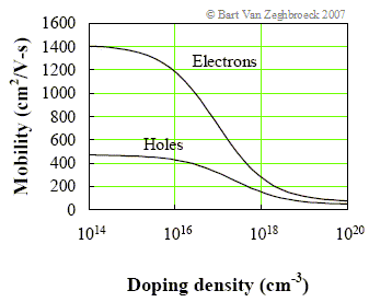 |
| Figure 2.7.3 : | Electron and hole mobility versus doping density for silicon.  |
The electron mobility and hole mobility have a similar doping dependence: For low doping concentrations, the mobility is almost constant and is primarily limited by phonon scattering. At higher doping concentrations, the mobility decreases due to ionized impurity scattering with the ionized doping atoms. The actual mobility also depends on the type of dopant. Figure 2.7.3 is for phosphorous and boron doped silicon. |
Note that the mobility is linked to the total number of ionized impurities or the sum of the donor and acceptor densities. The free carrier density, as described in section 2.6.4.1 is to first order related to the difference between the donor and acceptor concentration. |
The minority carrier mobility also depends on the total impurity density. The minority-carrier mobility can be approximated by the majority-carrier mobility in a material with the same number of impurities. |
The mobility at a particular doping density is obtained from the following empiric expression: |
 | (2.7.10) |
where μmin, μmax, α and Nr are fit parameters. These parameters for arsenic, phosphorous and boron doped silicon are provided in Table 2.7.2. |
 |
| Table 2.7.2 : | Parameters for calculation of the mobility as a function of the doping density |
The resulting mobilities in units of cm2/V-s are listed for different doping densities in Table 2.7.3. |
 |
| Table 2.7.3 : | Mobility in silicon for different dopants and doping densities |
The conductivity of a material is defined as the current density divided by the applied electric field. Since the current density equals the product of the charge of the mobile carriers, their density and velocity as described by equations (2.7.2a) and (2.7.2b), it can be expressed as a function of the electric field using the mobility. To include the contribution of electrons as well as holes to the conductivity, we add the current density due to holes to that of the electrons, or: |
 | (2.7.11) |
The conductivity due to electrons and holes is then obtained from: |
 | (2.7.12) |
The resistivity is defined as the inverse of the conductivity, namely: |
 | (2.7.13) |
The resulting resistivity as calculated with the expression above is shown in Figure 2.7.4. |
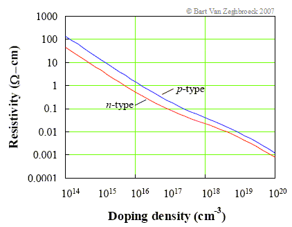 |
| Figure 2.7.4: | Resistivity of n-type and p-type silicon versus doping density.  |
The sheet resistance concept is used to characterize both wafers and thin doped layers, since it is typically easier to measure the sheet resistance rather than the resistivity of the material. The sheet resistance of a uniformly-doped layer with resistivity, ρ, and thickness, t, is given by their ratio: |
 | (2.7.14) |
While the unit of the sheet resistance is Ohms, one refers to it as Ohms per square. This nomenclature comes in handy when the resistance of a rectangular piece of material with length, L, and width W must be obtained. It equals the product of the sheet resistance and the number of squares or: |
 | (2.7.15) |
where the number of squares equals the length divided by the width. Figure 2.7.5 provides, as an example, the sheet resistance of a 14 mil thick silicon wafer for both n-type and p-type silicon. |
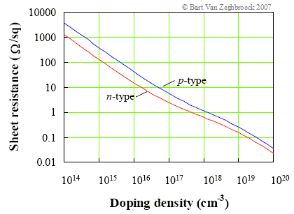 |
| Figure 2.7.5: | Sheet resistance of a 14 mil thick n-type and p-type silicon wafer versus doping density.  |
| Example 2.9 | A piece of silicon doped with arsenic (Nd = 1017 cm-3) is 100 μm long, 10 μm wide and 1 μm thick. Calculate the resistance of this sample when contacted one each end. |
| Solution | The resistivity of the silicon equals:
where the mobility was obtained from Table 2.7.3. The resistance then equals:
An alternate approach is to first calculate the sheet resistance, Rs:
From which one then obtains the resistance:
|
Next, we generalize the concept of the sheet resistance to a semiconductor layer with non-uniform doping as illustrated with Figure 2.7.6. |
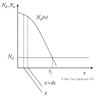 |
| Figure 2.7.6: | Non-uniform doping distribution. |
The doping profile is representative of a diffused and/or ion-implanted p-type layer in a uniformly doped n-type substrate. The metallurgical junction depth, xj, occurs when the two doping densities are equal. The sheet resistance of the section with width, dx, is given by: |
 | (2.7.16) |
Where both the mobility, μp(x), and hole density, p(x), are dependent on position. The sheet resistance of the whole layer is the parallel resistance of all slices with width dx between zero and xj, resulting in: |
 | (2.7.17) |
where |
2.7.3. Velocity saturation |      |
The linear relationship between the average carrier velocity and the applied field breaks down when high fields are applied. As the electric field is increased, the average carrier velocity and the average carrier energy increases as well. When the carrier energy increases beyond the optical phonon energy, the probability of emitting an optical phonon increases abruptly. This mechanism causes the carrier velocity to saturate with increasing electric field. For carriers in silicon and other materials, which do not contain accessible higher bands, the velocity versus field relation increases monotonically as shown in Figure 2.7.7a. |
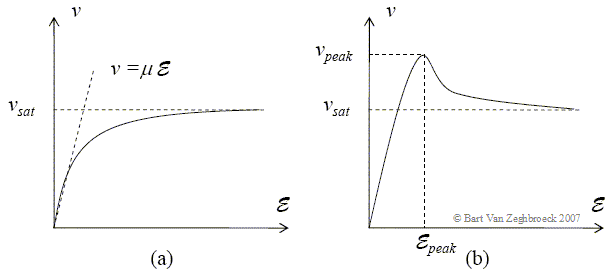 |
| Figure 2.7.7: | Velocity-field relation for a) materials without accessible higher bands such as silicon and b) materials with an accessible higher band such as GaAs. |
For those materials the velocity-field relation can be described by: |
 | (2.7.18) |
The maximum obtainable velocity, vsat, is referred to as the saturation velocity. |
The analysis is more complex for materials such as GaAs and InP, which contain multiple closely spaced conduction band minima. Electrons originating in the lowest Γ minimum accelerate under high field conditions and gain enough energy to transfer to the X or L minima. Since the density of states in the X and L minima is much higher because of the higher effective mass, the probability that the electron transfers back into the Γ minimum is small because of the small number of available states. The electrons therefore remain in the higher minima as long as the electric field exceeds the peak field. The corresponding velocity initially increases with increasing applied electric field. However as carriers transfer to the higher minimum with a higher effective mass, the average mobility and carrier velocity decrease. This causes a distinct peak in the velocity field curve as shown in Figure 2.7.7b. Such velocity-field curves are therefore characterized by the peak velocity, vpeak, and the peak field, Epeak, in addition to the mobility, μ, and the saturation velocity, vsat. |
A first estimate of the saturation velocity, vsat, of a material can be obtained by calculating the carrier velocity when it reaches an energy equal to the optical phonon energy. |
 | (2.7.19) |
While this equation can at best provide a rough estimate of the actual saturation velocity, it does indicate the right trend. Materials with a small effective mass and high optical phonon energy are more likely to have a high saturation velocity. Materials with multiple band minima can have a rather low saturation velocity, relative to the peak velocity, if the carriers in the higher minima have a larger effective mass. |
2.7.4. Carrier diffusion |      |
Carrier diffusion is due to the thermal energy, kT, which causes the carriers to move at random even when no field is applied. This random motion does not yield a net flow of carriers nor does it yield a net current in material with a uniform carrier density since any carrier which leaves a specific location is on average replace by another one. However if a carrier gradient is present, the diffusion process will even out the carrier density variations: carriers diffuse from regions where the density is high to regions where the density is low. The diffusion process is not unlike the motion of sand on a vibrating table; hills as well as valleys are smoothed out over time. |
In this section we will first derive the expression for the current due to diffusion and then combine it with the drift current to obtain the total drift-diffusion current. |
The derivation is based on the basic notion that carriers at non-zero temperature (Kelvin) have an additional thermal energy, which equals kT/2 per degree of freedom. It is the thermal energy, which drives the diffusion process. At T = 0 K there is no diffusion. |
The reader should recognize that the random nature of the thermal energy would normally require a statistical treatment of the carriers. Instead we will use average values to describe the process. Such approach is justified on the basis that a more elaborate statistical approach yields the same results. To further simplify the derivation, we will derive the diffusion current for a one-dimensional semiconductor in which carriers can only move along one direction. |
We now introduce the average values of the variables of interest, namely the thermal velocity, vth, the collision time, τc, and the mean free path, l. The thermal velocity is the average velocity of the carriers going in the positive or negative direction. The collision time is the time during which carriers will move with the same velocity before a collision occurs with an atom or with another carrier. The mean free path is the average length a carrier will travel between collisions. These three averages are related by: |
 | (2.7.20) |
Consider now the situation illustrated with Figure 2.7.7. |
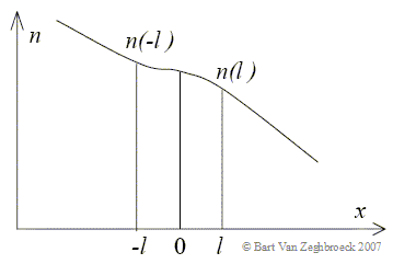 |
| Figure 2.7.8: | Carrier density profile used to derive the diffusion current expression |
Shown is a variable carrier density, n(x). Of interest are the carrier densities which are one mean free path away from x = 0, since the carriers, which will arrive at x = 0 originate either at x = -l or x = l. The flux at x = 0 due to carriers that originate at x = -l and move from left to right equals: |
 | (2.7.21) |
where the factor 1/2 is due to the fact that only half of the carriers move to the left while the other half moves to the right. The flux at x = 0 due to carriers that originate at x = +l and move from right to left, equals: |
 | (2.7.22) |
The total flux of carriers moving from left to right at x = 0 therefore equals: |
 | (2.7.23) |
Where the flux due to carriers moving from right to left is subtracted from the flux due to carriers moving from left to right. Given that the mean free path is small we can write the difference in densities divided by the distance between x = -l and x = l as the derivative of the carrier density: |
 | (2.7.24) |
The electron diffusion current equals this flux times the charge of an electron, or: |
 | (2.7.25) |
We now replace the product of the thermal velocity, vth, and the mean free path, l, by a single parameter, namely the diffusion constant, Dn, so that: |
 | (2.7.26) |
Repeating the same derivation for holes yields: |
 | (2.7.27) |
We now further explore the relation between the diffusion constant and the mobility. At first, it seems that there should be no relation between the two since the driving force is distinctly different: diffusion is caused by thermal energy while an externally applied field causes drift. However one essential parameter in the analysis, namely the collision time, τc, should be independent of what causes the carrier motion. |
We now combine the relation between the velocity, mean free path and collision time, |
 | (2.7.28) |
with the result from thermodynamics, stating that electrons carry a thermal energy which equals kT/2 for each degree of freedom. Applied to a one-dimensional situation, this leads to: |
 | (2.7.29) |
We use equations 2.7.2 and 2.7.2 to rewrite the product of the thermal velocity and the mean free path as a function of the carrier mobility: |
 | (2.7.30) |
Using the definition of the diffusion constant we then obtain the following expressions which are often referred to as the Einstein relations: |
 | (2.7.31) |
 | (2.7.32) |
| Example 2.10 | The hole density in an n-type silicon wafer (Nd = 1017 cm-3) decreases linearly from 1014 cm-3 to 1013 cm-3 between x = 0 and x = 1 μm. Calculate the hole diffusion current density. |
| Solution | The hole diffusion current density equals:
where the diffusion constant was calculated using the Einstein relation:
and the hole mobility in the n-type wafer was obtained from Table 2.7.3 as the hole mobility in a p-type material with the same doping density. |
The total electron current is obtained by adding the current due to diffusion to the drift current, resulting in: |
 | (2.7.33) |
and similarly for holes: |
 | (2.7.34) |
The total current is the sum of the electron and hole current densities multiplied with the area, A, perpendicular to the direction of the carrier flow: |
 | (2.7.35) |
Whenever drift or diffusion of carriers occurs, the semiconductor is no longer in thermal equilibrium. As a result we can no longer use a constant Fermi energy throughout the semiconductor. We therefore generalize the concept of the Fermi energy by allowing the Fermi energy to vary throughout the material and by assigning a different Fermi energy, namely the Quasi-Fermi energies, Fn and Fp, to electrons and holes. This approach is based on the notion that the electron and hole distributions van still be approximated with the same distribution function, but that electrons are no longer in thermal equilibrium with holes. The equations for the carrier densities are then: |
 | (2.7.36) |
 | (2.7.37) |
The physical interpretation of the quasi-Fermi energies can be clarified by inserting equations (2.7.36) and (2.7.37) into the expressions for the electron and hole current density, (2.7.33) and (2.7.34): |
 | (2.7.38) |
 | (2.7.39) |
which can be simplified by rewriting the gradient of the intrinsic energy as function of the electric field using (2.3.8), resulting in: |
 | (2.7.40) |
 | (2.7.41) |
From this equation, we conclude that the gradient of the quasi-Fermi energy represents the total force acting on the carriers including both the force due to the applied electric field and the force due to the carrier gradient. |
2.7.5. The Hall Effect |      |
The Hall effect describes the behavior of the free carriers in a semiconductor when applying an electric as well as a magnetic field. The experimental setup shown in Figure 2.7.8, depicts a semiconductor bar with a rectangular cross section and length L. A voltage Vx is applied between the two contacts, resulting in a field along the x-direction. The magnetic field is applied in the z-direction. |
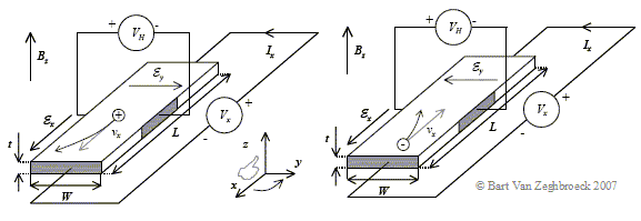 |
| Figure 2.7.9: | Hall setup and carrier motion for a) holes and b) electrons. |
As shown in Figure 2.7.8a), the holes move in the positive x-direction. The magnetic field causes a force to act on the mobile particles in a direction dictated by the right hand rule. As a result there is a force, Fy, along the positive y-direction, which moves the holes to the right. In steady state this force is balanced by an electric field, |
The behavior of electrons is shown in 2.7.7b). The electrons travel in the negative x-direction. Therefore the force, Fy, is in the positive y-direction due to the negative charge and the electrons move to the right, just like holes. The balancing electric field, |
To calculate the Hall field, we first calculate the Lorentz force acting on the free carriers: |
 | (2.7.42) |
We now assume that the carriers can only flow along the x-direction and label their velocity vx. The Lorentz force then becomes: |
 | (2.7.43) |
Since the carriers only flow along the x-direction, the net force must be zero along the y and z direction. As a result, the electric field is zero along the z direction and: |
 | (2.7.44) |
which provides a relation between the electric field along the y-direction and the applied magnetic field. Equation (2.7.36) can also be rewritten as a function of the current density, Jx, using (2.7.2b), yielding: |
 | (2.7.45) |
This electric field is called the Hall field. The Hall coefficient, RH, is defined as the Hall field divided by the current density, Jx, and magnetic field, Bz: |
 | (2.7.46) |
Once the Hall coefficient is obtained one easily finds the hole density: |
 | (2.7.47) |
The carrier mobility can also be extracted from the Hall coefficient: |
 | (2.7.48) |
Where ρ is the resistivity of the semiconductor. |
Alternatively, one can calculate the Hall coefficient from the measured current, Ix, and measured voltage, VH: |
 | (2.7.49) |
A measurement of the Hall voltage is often used to determine the type of semiconductor (n-type or p-type) the free carrier density and the carrier mobility. Repeating the measurement at different temperatures allows one to measure the free carrier density as well as the mobility as a function of temperature. Since the measurement can be done on a small piece of uniformly doped material it is by far the easiest measurement to determine the carrier mobility. It should be noted that the scattering mechanisms in the presence of a magnetic field are different and that the measured Hall mobility can differ somewhat from the drift mobility. A measurement of the carrier density versus temperature provides information regarding the ionization energies of the donors and acceptor that are present in the semiconductor as described in section 2.6.4.4. While the interpretation of the Hall measurement is straightforward in the case of a single dopant, multiple types of impurities and the presence of electrons and holes can make the interpretation non-trivial. |
| Boulder, 2022 |