7.6.1. Channel length modulation |   |
Channel length modulation in a MOSFET is caused by the increase of the depletion layer width at the drain as the drain voltage is increased. This leads to a shorter channel length and an increased drain current. An example is shown in Figure 7.6.1. The channel-length-modulation effect typically increases in small devices with low-doped substrates. An extreme case of channel length modulation is punch through where the channel length reduces to zero. Proper scaling can reduce channel length modulation, namely by increasing the doping density as the gate length is reduces. |
 |
| Figure 7.6.1: | Current-Voltage characteristics of a MOSFET with and without channel length modulation. (Nd = 1017 cm-3, L = 1 μm)  |
7.6.2. Drain induced barrier lowering | |
Drain induced barrier lowering (DIBL) is the effect the drain voltage on the output conductance and measured threshold voltage. This effect occurs in devices where only the gate length is reduced without properly scaling the other dimensions. It is observed as a variation of the measured threshold voltage with reduced gate length. The threshold variation is caused by the increased current with increased drain voltage as the applied drain voltage controls the inversion layer charge at the drain, thereby competing with the gate voltage. This effect is due to the two-dimensional field distribution at the drain end and can typically be eliminated by properly scaling the drain and source depths while increasing the substrate doping density. |
7.6.3. Punch through | |
Punch through in a MOSFET is an extreme case of channel length modulation where the depletion layers around the drain and source regions merge into a single depletion region. The field underneath the gate then becomes strongly dependent on the drain-source voltage, as is the drain current. Punch through causes a rapidly increasing current with increasing drain-source voltage. This effect is undesirable as it increases the output conductance and limits the maximum operating voltage of the device |
7.6.4. Sub-threshold current | |
The basic assumption of the MOS capacitor analysis in section 6.3.2 is that no inversion layer charge exists below the threshold voltage. This leads to zero current below threshold. The actual sub-threshold current is not zero but reduces exponentially below the threshold voltage as: |
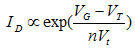 | (7.6.1) |
with |
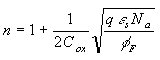 | (7.6.2) |
The sub-threshold behavior is critical for dynamic circuits since one needs to ensure that no charge leaks through transistors biased below threshold. |
The charge density below threshold can be expressed as: |
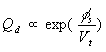 | (7.6.3) |
Where the surface potential, φs, is related to the gate voltage by: |
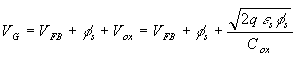 | (7.6.4) |
The gate voltage, VG, is therefore related to the surface potential, φs, by: |
 | (7.6.5) |
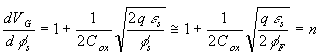
Where the surface potential below threshold was approximated to its value, 2 φF, at threshold. The sub-threshold current therefore equals: |
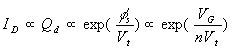 | (7.6.6) |
7.6.5. Field dependent mobility | |
The mobility is the inversion layer is distinctly lower than in bulk material. This is due to the fact the electron wavefunction extends into the oxide and the carrier mobility is lowered due to the lower mobility in the oxide. Higher electric fields at the surface - as typically obtained in scaled devices - push the electron wavefunction even more into the oxide yielding a field dependent mobility. The mobility at the surface, μsurface, varies with the electric field, |
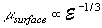 | (7.6.7) |
7.6.6. Avalanche breakdown and parasitic bipolar action | |
As the electric field in the channel is increased, avalanche breakdown occurs in the channel at the drain. This avalanche breakdown increases the current as in a p-n diode (see section 4.5.3 and 2.8). In addition, there is parasitic bipolar action taking place. Holes generated by the avalanche breakdown move from drain to source underneath the inversion layer. This hole current forward biases the source-bulk p-n diode so that now also electrons are injected as minority carriers into the p-type substrate underneath the inversion layer. These electrons arrive at the drain and again create more electron-hole pairs through avalanche multiplication. The positive feedback between the avalanche breakdown and the parasitic bipolar action results in breakdown at lower drain voltage. |
7.6.7. Velocity saturation | |
As devices are reduced in size, the electric field typically also increases and the carriers in the channel have an increased velocity. However at high fields there is no longer a linear relation between the electric field and the velocity as the velocity gradually saturates reaching the saturation velocity. This velocity saturation is caused by the increased scattering rate of highly energetic electrons, primarily due to optical phonon emission. This effect increases the transit time of carriers through the channel. In sub-micron MOSFETs one finds that the average electron velocity is larger than in bulk material so that velocity saturation is not quite as much of a restriction as initially thought. |
7.6.8. Oxide Breakdown | |
As the gate-oxide is scaled down, breakdown of the oxide and oxide reliability becomes more of a concern. Higher fields in the oxide increase the tunneling of carriers from the channel into the oxide. These carriers slowly degrade the quality of the oxide and lead over time to failure of the oxide. This effect is referred to as time dependent destructive breakdown (TDDB). |
Oxides other than silicon dioxide have been considered as alternate oxides and are typically referred to as high-k dielectrics. These oxides have a larger dielectric constant so that the same gate capacitance can be obtained with a thicker oxide. The challenge is to obtain the same stability, reliability and breakdown voltage as silicon dioxide. Oxides of interest include Al2O3, ZrO and TiO. |
7.6.9. Scaling | |
The reduction of the dimensions of a MOSFET has been has dramatic during the last three decades. Starting at a minimum feature length of 10 μm in the 1970's the gate length was gradually reduced to 0.15 μm minimum feature size in 2000, resulting in a 13% reduction per year. Proper scaling of MOSFET however requires not only a size reduction of the gate length and width. It also requires a reduction of all other dimensions including the gate/source and gate/drain alignment, the oxide thickness and the depletion layer widths. Scaling of the depletion layer widths also implies scaling of the substrate doping density. |
Two types of scaling are common: constant field scaling and constant voltage scaling. Constant field scaling yields the largest reduction in the power-delay product of a single transistor. However, it requires a reduction in the power supply voltage as one decreases the minimum feature size. Constant voltage scaling does not have this problem and is therefore the preferred scaling method since it provides voltage compatibility with older circuit technologies. The disadvantage of constant voltage scaling is that the electric field increases as the minimum feature length is reduced. This leads to velocity saturation, mobility degradation, increased leakage currents and lower breakdown voltages. |
The scaling of MOSFET device parameters is illustrated by Table 7.6.1 where constant field, constant voltage and constant voltage scaling in the presence of velocity saturation are compared. |
 |
| Table 7.6.1 : | Comparison of the effect of scaling on MOSFET device parameters. Compared are constant field scaling, constant voltage scaling and constant voltage scaling in the presence of velocity saturation. |
Boulder, December 2004 |
 , in the following way: