7.7.1. MOSFET fabrication process


The MOSFET circuit technology has dramatically changed over the last three decades. Starting with a ten-micron pMOS process with an aluminum gate and a single metallization layer around 1970, the technology has evolved into a tenth-micron self-aligned-gate CMOS process with up to five metallization levels. The transition from dopant diffusion to ion implantation, from thermal oxidation to oxide deposition, from a metal gate to a poly-silicon gate, from wet chemical etching to dry etching and more recently from aluminum (with 2% copper) wiring to copper wiring has provided vastly superior analog and digital CMOS circuits. |
7.7.1. MOSFET fabrication process |      |
A quick look at the history of the MOSFET fabrication process reveals that it has evolved significantly over the years. Around 1970, pMOS circuits with aluminum gate metal and wiring were dominant. The corresponding steps of a typical pMOSFET fabrication process steps are listed in Table 7.7.1. |
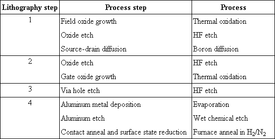 |
| Table 7.7.1: | pMOS process steps |
The primary problem at the time was threshold voltage control. Positively charged ions in the oxide decreased the threshold voltage of the devices. p-type MOSFETs were therefore the device of choice despite the lower hole mobility, since they would still be enhancement-type devices even when charge was present. Circuits were still operational at somewhat higher power supply voltages despite the presence of some residual charge in the oxide. |
Thermal oxidation of the silicon in an oxygen or water vapor atmosphere provided a quality gate oxide with easily controlled thickness. The same process was also used to provide a high-temperature mask for the diffusion process and a passivation and isolation layer. Some people claim that the quality and versatility of siliconŐs oxide made silicon the preferred semiconductor over germanium. |
The oxide was easily removed in hydrofluoric acid (HF), without removing the underlying silicon, thanks to the high selectivity if the etch. |
Aluminum was evaporated over the whole wafer and then etched yielding both the gate metal and the metal wiring connecting the devices. A small amount of copper (~2%) was added to make the aluminum more resistant to electromigration. Electromigration is the movement of atoms due to the impact with the electrons carrying the current through the wire. This effect can cause open circuits and is therefore a well-known reliability problem. It typically occurs at points where the local current density is very high, in narrow wires, at corners or when crossing an oxide step. The addition of a small amount of copper provides a more rigid structure within the aluminum and eliminates the effect. |
Annealing the metal in a nitrogen/hydrogen (N2/H2) ambient was used to improve the metal-semiconductor contact and to reduce the surface state density at the semiconductor/gate-oxide interface. |
Since then the fabrication process has changed as illustrated with Table 7.7.2. Most changes were introduced to provide superior performance, better reliability and higher yield. The most important change has been the reduction of the gate length. A gate length reduction provides a shorter transit time and hence a faster device. In addition, a gate length reduction is typically linked to a reduction of the minimum feature size and therefore yields smaller transistors as well as a larger number of transistors on a chip with a given size. As the technology improved, it was also possible to make larger chips, so that the number of transistors per chip increased even faster. At the same time, the wafer size was increased to accommodate the larger chips while reducing the loss due to partial chips at the wafer periphery. Larger wafers further reduce the cost per chip as more chips can be accommodated on a single wafer. |
The other changes can be split into process improvements and circuit improvements. The distinction is at times artificial, as circuit improvements typically require new processes. |
The key circuit improvement is the use of CMOS circuits, containing both nMOS and pMOS transistors. Early on, the pMOS devices were replaced with nMOS transistors because of the better electron mobility. Enhancement-mode loads were replaced for first by resistor loads and then by depletion-mode loads yielding faster logic circuits with larger operating margins. Analog circuits benefited in similar ways. The use of complementary circuits was first introduced by RCA but did not immediately catch on since the logic circuits were somewhat slower and larger than the then-dominant nMOS depletion logic. It was only when the number of transistors per chip became much larger that the inherent advantages of CMOS circuits became clear. CMOS circuits have a lower power dissipation and larger operating margin. They became the technology of choice as thousands of devices we integrated on a single chip. Today, the CMOS technology is the dominant technology in the IC industry as the ten-fold reduction of power dissipation largely outweighs the 30%-50% speed reduction and size increase. |
The process improvements can in turn be split into those aimed at improving the circuit performance and those improving the manufacturability and reliability. Again the split is somewhat artificial but it is beneficial to understand what factors affect the process changes. The latter group includes CVD deposition, ion implantation, RIE etching, sputtering, planarization and deuterium annealing. The process changes, which improve the circuit performance, are the self-aligned poly-silicon gate process, the silicide gate cap, LOCOS isolation, multilevel wiring and copper wiring. |
The self-aligned poly-silicon gate process was introduced before CMOS and marked the beginning of modern day MOSFETs. The self-aligned structure, as further discussed in section 7.7.2, is obtained by using the gate as the mask for the source-drain implant. Since the crystal damage caused by the high-energy ions must be annealed at high temperature (~800 C), an aluminum gate could no longer be used. Doped poly-silicon was found to be a very convenient gate material since it withstands the high anneal temperature and can be oxidized just like silicon. The self-aligned process lowers the parasitic capacitance between gate and drain and therefore improves the high-frequency performance and switching time. The addition of a silicide layer on top of the gate reduces the gate resistance while still providing a quality implant mask. The self-aligned process also reduced the transistor size and hence increased the density. The field oxide was replaced by a local oxidation isolation structure (LOCOS), where a Si3N4 layer is used to prevent the oxidation in the MOSFET region. This oxide provides an implant mask and contact hole mask yielding an even more compact device. |
Multilevel wiring is a necessity when one increases the number of transistors per chip. After all, the number of wires increases with the square of the number of transistors and the average wire length increase linearly with the chip size. While multilevel wiring simply consists of a series of metal wiring levels separated by insulators, the multilevel wiring has increasingly become a bottleneck in the fabrication of high-performance circuits. Planarization techniques, as discussed below, and the introduction of copper instead of aluminum-based metals have further increased the wiring density and lowered the wiring resistance. |
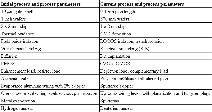 |
| Table 7.7.2: | MOS process changes and improvements |
Chemical vapor deposition (CVD) of insulating layers is now used instead of thermal oxidation since it does not consume the underlying silicon. Also, because there is no limit to the obtainable thickness and since materials other than SiO2 (for instance Si3N4) can be deposited. CVD deposition is also frequently used to deposit refractory metals such as tungsten. |
Ion implantation has replaced diffusion because of its superior control and uniformity. Dry etching including plasma etching, reactive ion etching (RIE) and ion beam etching has replaced wet chemical etching. These etch processes provide better etch rate uniformity and control as well as very pronounced anisotropic etching. The high etch rate selectivity of wet chemical etching is not obtained with these dry etch techniques, but are well compensated by the better uniformity. |
Sputtering of metals has completely replaced evaporation. Sputtering typically provides better adhesion and thickness control. It is also better suited to deposit refractory metals and silicides. |
Planarization is the process by which the top surface of the wafer is planarized after each step. The purpose of this planarization process is to provide a flat surface, so that fine-line lithography can be performed at all stages of the fabrication process. The planarization enables high-density multi-layer wiring levels. |
Deuterium anneal is a recent modification of the standard hydrogen anneal, which passivates the surface states. The change to deuterium was prompted because it is a heavier isotope of hydrogen. It chemically acts the same way but is less likely to be knocked out of place by the energetic carriers in the inversion layer. The use of deuterium therefore reduces the increase of the surface state density due to hot-electron impact. |
7.7.2. Poly-silicon gate technology |      |
An early improvement of the technology was obtained by using a poly-silicon gate. Such gate yields a compact self-aligned structure with better performance. The poly-silicon gate is used as a mask during the implantation so that the source and drain regions are self-aligned with respect to the gate. This self-alignment structure reduces the device size. In addition, it eliminates the large overlap capacitance between gate and drain, while maintaining a continuous inversion layer between source and drain. |
A further improvement of this technique is the use of a low-doped drain (LDD) structure. As an example we consider the structure shown in Figure 7.7.1. Here a first shallow implant is used to contact the inversion layer underneath the gate. The shallow implant causes only a small overlap between the gate and source/drain regions. After adding a sidewall to the gate a second deep implant is added to the first one. This deep implant has a low sheet resistance and adds a minimal series resistance. The combination of the two implants therefore yields a minimal overlap capacitance and low access resistance. |
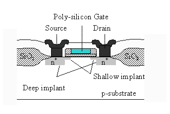 |
| Figure 7.7.1: | Cross-sectional view of a self-aligned poly-silicon gate transistor with LOCOS isolation |
Shown is also the local oxidation isolation (LOCOS). Typically, there would also be an additional field and channel implant. The field implant increases the doping density under the oxide and thereby increases the threshold voltage of the parasitic transistor formed by the metal wiring on top of the isolation oxide. The channel implant provides an adjustment of the threshold voltage of the transistors. The use of a poly-silicon gate has the disadvantage that the sheet resistance of the gate is much larger than that of a metal gate. This leads to high RC time-constants of long poly-silicon lines. Silicides (WSi, TaSi, CoSi etc.) or a combination of silicides and poly-silicon are used to reduce these RC delays. Also by using the poly-silicon only as gate material and not as a wiring level one can further eliminated such RC time delays. |
7.7.3. CMOS |      |
Complementary Metal-Oxide-Silicon circuits require an nMOS and pMOS transistor technology on the same substrate. To this end, an n-type well is provided in the p-type substrate. Alternatively one can use a p-well or both an n-type and p-type well in a low-doped substrate. The gate oxide, poly-silicon gate and source-drain contact metal are typically shared between the pMOS and nMOS technology, while the source-drain implants must be done separately. Since CMOS circuits contain pMOS devices, which are affected by the lower hole mobility, CMOS circuits are not faster than their all-nMOS counter parts. Even when scaling the size of the pMOS devices so that they provide the same current, the larger pMOS device has a higher capacitance. |
The CMOS advantage is that the output of a CMOS inverter can be as high as the power supply voltage and as low as ground. This large voltage swing and the steep transition between logic levels yield large operation margins and therefore also a high circuit yield. In addition, there is no power dissipation in either logic state. Instead the power dissipation occurs only when a transition is made between logic states. CMOS circuits are therefore not faster than nMOS circuits but are more suited for very/ultra large-scale integration (VLSI/ULSI). |
CMOS circuits have one property, which is very undesirable, namely latchup. Latchup occurs when four alternating p-type and n-type regions are brought in close proximity. Together they form two bipolar transistors, one npn and one pnp transistor. The base of each transistor is connected to the collector of the other, forming a cross-coupled thyristor-like combination (see also section 5.9.3). As a current is applied to the base of one transistor, the current is amplified by the transistor and provided as the base current of the other one. If the product of the current gain of both transistors is larger than unity, the current through both devices increases until the series resistances of the circuit limits the current. Latchup therefore results in excessive power dissipation and faulty logic levels in the gates affected. In principle, this effect can be eliminated by separating the n-type and p-type device. A more effective and less space-consuming solution is the use of trenches, which block the minority carrier flow. A deep and narrow trench is etched between all n-type and p-type wells, passivated and refilled with an insulating layer. |
7.7.4. MOSFET Memory |      |
MOSFET memory is an important application of MOSFETs. Memory chips contain the largest number of devices per unit area since the transistors are arranged in a very dense regular structure. The generic structure of a memory chip is shown in Figure 7.7.2. |
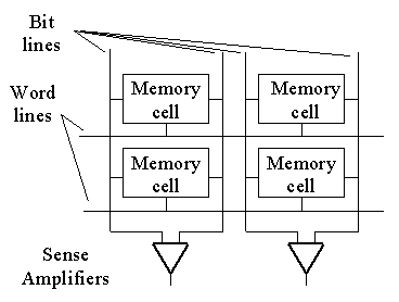 |
| Figure 7.7.2: | Arrangement of memory cells into an array |
A two dimensional array of memory cells, each containing a single bit, are connected through a series of word lines and bit lines. One row of cells is activated by changing the voltage on the corresponding word line. The information is then stored in the cell by applying voltages to the bit lines. During a read operation, the information is retrieved by sensing the voltage on the bit lines with a sense amplifier. A possible implementation of a static random access memory (SRAM) is shown in Figure 7.7.3. |
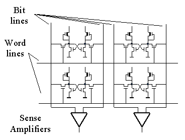 |
| Figure 7.7.3: | Static random access memory (SRAM) using a six-transistor cell. |
Each memory cell consists of a flip-flop and the cells are accessed through two pass transistors connected to the bit lines and controlled by the word line. Depletion mode transistors are shown here as load devices. A common alternate load is an amorphous silicon resistor. |
A simpler cell leading to denser memory chips is the dynamic random access memory (DRAM) shown in Figure 7.7.4. |
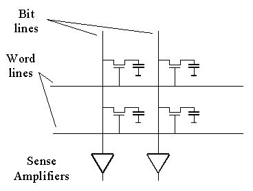 |
| Figure 7.7.4: | Dynamic random access memory (DRAM) using a one-transistor cell. |
The dynamic cell contains only a single transistor and capacitor. The cell is called dynamic since the information is stored as charge on the capacitor. This charge slowly leaks away so that the cell needs to be refreshed periodically. The reading process is also destructive since the storage capacitor is discharged as a voltage is applied to the word line. Therefore, one has to rewrite the information into all the cells of a given row after reading a single cell from that row. Despite these restrictions, dynamic memory chips represent the largest section of the memory market. The advantage of a higher storage density outweighs all other considerations. Process advances such as the use of a vertical trench, have further increased the density of dynamic memory chips. |
As an example we now consider the dynamic memory cell shown in Figure 7.7.5. Shown are the top view and cross-sectional view. The figure illustrates how compact the cell can be by using the gate as the word line of the array and by using a trench capacitor. Also note that the drain of the transistor and one side of the capacitor are merged into one n-type region. The bit lines shown in the top view are placed next to the transistor for clarity. Actual memory cells have the bit lines on top of the transistors as shown in the cross-sectional view. More recent memory cells even have the transistor buried in the trench together with the capacitor. |
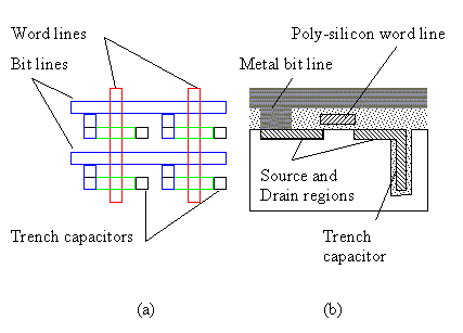 |
| Figure 7.7.5: | Dynamic random access memory (DRAM) using a one-transistor cell. (a) top view of four cells and (b) cross-sectional view of one cell. |
A critical issue when scaling dynamic memory circuits is the capacitance of the storage capacitor. Scaling of all dimensions would yield a smaller value of the capacitor. However, larger arrays, made possible by scaling the device size, require a larger capacitance. After all, the critical operation in a dynamic memory is the read-out. During read-out, the memory capacitor is connected to the bit line and the charge is now distributed between the memory cell capacitance, the bit line capacitance and the parasitic capacitance of all the devices connected to the bit line. The remaining voltage on the bit line therefore depends on the ratio of the cell capacitance to that of the bit line and connected elements. In large memory chips the voltage would become unacceptably low if the memory capacitance would be scaled down with all other device dimensions. Instead the capacitance of the memory capacitor is kept almost constant from one generation to the next at a value around 1 fF. This value corresponds to the storage of 25,000 electrons at a voltage of 5 V and results in a bit line voltage of a few millivolts. |
Boulder, December 2004 |