7.8.1. LDMOS |   |
The Laterally Diffused MOSFET (LDMOS) is an asymmetric power MOSFET designed for low on-resistance and high blocking voltage. These features are obtained by creating a diffused p-type channel region in a low-doped n-type drain region. The low doping on the drain side results in a large depletion layer with high blocking voltage. The channel region diffusion can be defined with the same mask as the source region, resulting in a short channel with high current handling capability. The relatively deep p-type diffusion causes a large radius of curvature at the edges, which eliminates the edge effects discussed in section 4.5.2. While the deviceŐs name implies that the fabrication requires a diffusion, the dopants can just as well be implanted and annealed. Diffusion can be used in addition to further increase the junction depth and radius of curvature. |
A typical structure is presented in Figure 7.8.1. The device can be fabricated by diffusion as well as ion implantation. The p-type region is formed first, followed by shallow p+ and n+ regions. The n+ regions provide both source and drain contact regions. The p+-region contacts the p-type body, which is typically shorted to the source, thereby eliminating the body effect. |
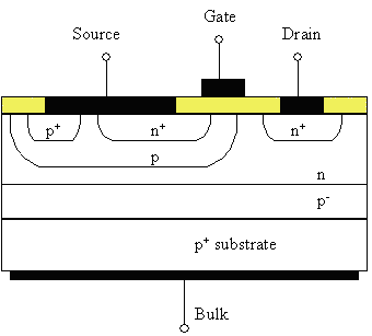 |
| Figure 7.8.1: | Cross-section of a Laterally Diffused MOSFET (LDMOS) structure. |
The LDMOS structure combines a short channel length with high breakdown voltage as desired for high power RF amplifiers in numerous applications. This device is currently the device of choice for RF power amplifiers in the base stations of wireless communications systems as well as numerous UHF and L-band power amplifiers in broadcast, communication and radar systems. |
7.8.2. VMOS Transistors and UMOS | |
The VMOS transistor, named after the V-shaped groove, is a vertical MOSFET with high current handling capability as well as high blocking voltage. It consists of a double diffused n+/p layer, which is cut by a V-shaped groove as shown in Figure 7.8.2.a. The V-groove is easily fabricated by anisotropically etching a (100) silicon surface using a concentrated KOH solution. The V-groove is then coated with a gate oxide, followed by the gate electrode. As the V-groove cuts through the double diffused layer, it creates two vertical MOSFETs, one on each side of the groove. The combination of the V-groove with the double diffused layers results in a short gatelength, which is determined by the thickness of the p-type layer. The vertical structure allows the use of a low-doped drain region, which results in a high blocking voltage. |
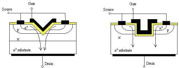 |
| Figure 7.8.2: | Cross-section of two vertical MOSFET structures: a) VMOS and b) UMOS. |
Another alternate structure is the UMOS structure. A vertical trench is etched though the double diffused layer, again resulting in two vertical MOSFETs. |
Either one of these vertical structures can further be combined with the HEXFET layout. This layout resembles a honeycomb structure in which the hexagonal areas are source areas, while the gate metal is located on the perimeters. |
7.8.3. Insulated Gate Bipolar Transistors (IGBTs) | |
The Insulated Gate Bipolar Transistor or IGBT for short combines the high dc current gain of a MOSFET with the high current handling capability and high blocking voltage of a BJT in a surprisingly simple structure, like as the one shown in Figure 7.8.3. At first glance, the vertical structure looks like that of a regular vertical MOSFET structure. However a closer look reveals a p+ substrate rather than an n+ substrate. To further analyze this structure we use the equivalent circuit, which contains the lateral MOSFET as well as the pnp BJT as formed by the bottom three layers. One should note that the p-type collector of the pnp BJT and the n-type source of the nMOSFET share the same metal contact. Also, that the drain region of the nMOSFET is the buried n-type layer, which is also the n-type base of the pnp BJT. The electrons originating from the n+ source flow laterally underneath the gate and then flow down in the buried n-type region, thereby supplying the gate current of the pnp BJT. Since the gate current is provided locally, the emitter current will be concentrated around the same area. Note that under typical operation the collector would be grounded while a positive voltage is applied to the emitter. Therefore, this device can be connected in a switching circuit just like an npn BJT with the important distinction that no gate current is required to maintain the on-state current. |
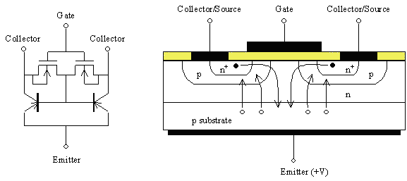 |
| Figure 7.8.3: | Insulated Gate Bipolar Transistor (IGBT): a) equivalent circuit and b) device cross-section. |
Boulder, December 2004 |