Current mechanisms through materials, which do not contain free carriers, can be distinctly different from those in doped semiconductors or metals. The following section discusses Fowler-Nordheim Tunneling, Poole-Frenkel emission, Space charge effects as well as Ballistic transport. While these current mechanisms are not related to Metal-Semiconductor junctions, they are presented here since they represent unipolar current mechanisms. |
3.9.1 Fowler-Nordheim tunneling |   |
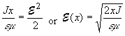
Fowler-Nordheim tunneling has been studied extensively in Metal-Oxide-Semiconductor structures where it has been shown to be the dominant current mechanism, especially for thick oxides. The basic idea is that quantum mechanical tunneling from the adjacent conductor into the insulator limits the current through the structure. Once the carriers have tunneled into the insulator they are free to move within the valence or conduction band of the insulator. The calculation of the current is based on the WKB approximation (as derived section 3.3.4) yielding the following relation between the current density, JFN, and the electric field in the oxide, |
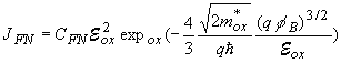 | (3.9.1) |
where fB is the barrier height at the conductor/insulator interface. |
To check for this current mechanism, experimental I-V characteristics are typically plotted as ln(JFN/ |
It is this type of measurement, which has yielded experimental values for the conduction band difference between different metals and silicon dioxide. It is important to note that carriers must tunnel through the insulator, which requires: |
 | (3.9.2) |
as is typically the case for thick oxides and high electric fields. |
3.9.2 Poole-Frenkel emission | |
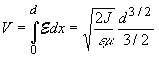
The expression for Fowler-Nordheim tunneling implies that carriers are free to move through the insulator. Whereas this is indeed the case in thermally grown silicon dioxide it is frequently not so in deposited insulators, which contain a high density of structural defects. Silicon nitride (Si3N4) is an example of such material. The structural defects cause additional energy states close to the band edge, called traps. These traps restrict the current flow because of a capture and emission process, thereby becoming the dominant current mechanism. The current is a simple drift current described by |
 | (3.9.3) |
while the carrier density depends exponentially on the depth of the trap, which is corrected for the electric field |
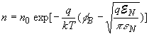 | (3.9.4) |
The total current then equals: |
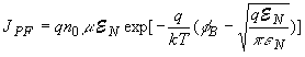 | (3.9.5) |
The existence of a large density of shallow traps in CVD silicon nitride makes Poole-Frenkel emission a frequently observed and well-characterized mechanism. |
3.9.3 Space charge limited current | |
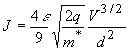
Both Fowler-Nordheim tunneling and Poole-Frenkel emission mechanism yield very low current densities with correspondingly low carrier densities. For structures where carriers can readily enter the insulator and freely flow through the insulator one finds that the resulting current and carrier densities are much higher. The high density of these charged carriers causes a field gradient, which limits the current density. This situation occurs in lowly doped semiconductors and vacuum tubes. We start from an expression for the drift current and Gauss's law (where we assume that the insulator contains no free carriers if no current flows) |
 | (3.9.6) |
 | (3.9.7) |
Positively charged holes are assumed in this derivation, but the result equally holds for electrons. Next we can eliminate the carrier density, p, yielding: |
 | (3.9.8) |
Integrating this expression from 0 to x, while we assuming the electric field to be zero at x = 0 one obtains: |
 | (3.9.9) |
integrating once again from x = 0 to x = d with V(0) = V and V(d) = 0, one finds: |
 | (3.9.10) |
from which one obtains the expression for the space-charge-limited current: |
 | (3.9.11) |
3.9.4 Ballistic Transport in insulators | |
Ballistic transport is carrier transport without scattering or any other mechanism, which would cause a loss of energy. Combining energy conservation, current continuity and Gauss's law one finds the following current-voltage relation: |
 | (3.9.12) |
where d is the thickness of the insulator and m* is the effective mass of the carriers. |
 ox:
ox: