
The electrostatic analysis of a p-n diode is of interest since it provides knowledge about the charge density and the electric field in the depletion region. It is also required to obtain the capacitance-voltage characteristics of the diode. The analysis is very similar to that of a metal-semiconductor junction (section 3.3). A key difference is that a p-n diode contains two depletion regions of opposite type. |
4.3.1. General discussion - Poisson's equation |   |
The general analysis starts by setting up Poisson's equation: |
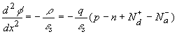 | (4.3.1) |
where the charge density, r, is written as a function of the electron density, the hole density and the donor and acceptor densities. To solve the equation, we have to express the electron and hole density, n and p, as a function of the potential, f, yielding: |
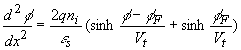 | (4.3.2) |
with |
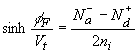 | (4.3.3) |
where the potential is chosen to be zero in the n-type region, far away from the p-n interface. |
This second-order non-linear differential equation (4.3.2) cannot be solved analytically. Instead we will make the simplifying assumption that the depletion region is fully depleted and that the adjacent neutral regions contain no charge. This full depletion approximation is the topic of the next section. |
4.3.2. The full-depletion approximation | |
The full-depletion approximation assumes that the depletion region around the metallurgical junction has well-defined edges. It also assumes that the transition between the depleted and the quasi-neutral region is abrupt. We define the quasi-neutral region as the region adjacent to the depletion region where the electric field is small and the free carrier density is close to the net doping density. |
The full-depletion approximation is justified by the fact that the carrier densities change exponentially with the position of the Fermi energy relative to the band edges. For example, as the distance between the Fermi energy and the conduction band edge is increased by 59 meV, the electron concentration at room temperature decreases to one tenth of its original value. The charge in the depletion layer is then quickly dominated by the remaining ionized impurities, yielding a constant charge density for uniformly doped regions. |
We will therefore start the electrostatic analysis using an abrupt charge density profile, while introducing two unknowns, namely the depletion layer width in the p-type region, xp, and the depletion region width in the n-type region, xn. The sum of the two depletion layer widths in each region is the total depletion layer width xd, or: |
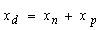 | (4.3.4) |
From the charge density, we then calculate the electric field and the potential across the depletion region. A first relationship between the two unknowns is obtained by setting the positive charge in the depletion layer equal to the negative charge. This is required since the electric field in both quasi-neutral regions must be zero. A second relationship between the two unknowns is obtained by relating the potential across the depletion layer width to the applied voltage. The combination of both relations yields a solution for xp and xn, from which all other parameters can be obtained. |
4.3.3. Full depletion analysis | |
Once the full-depletion approximation is made, it is easy to find the charge density profile: It equals the sum of the charges due to the holes, electrons, ionized acceptors and ionized holes: |
 | (4.3.5) |
where it is assumed that no free carriers are present within the depletion region. For an abrupt p-n diode with doping densities, Na and Nd, the charge density is then given by: |
 | (4.3.6) |
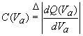
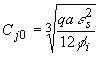
This charge density, r, is shown in Figure 4.3.1 (a). |
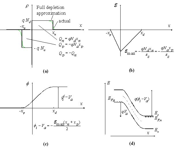 |
| Figure 4.3.1: | (a) Charge density in a p-n junction, (b) Electric field, (c) Potential and (d) Energy band diagram |
As can be seen from Figure 4.3.1 (a), the charge density is constant in each region, as dictated by the full-depletion approximation. The total charge per unit area in each region is also indicated on the figure. The charge in the n-type region, Qn, and the charge in the p-type region, Qp, are given by: |
 | (4.3.7) |
 | (4.3.8) |
The electric field is obtained from the charge density using Gauss's law, which states that the field gradient equals the charge density divided by the dielectric constant or: |
 | (4.3.9) |
The electric field is obtained by integrating equation (4.3.9). The boundary conditions, consistent with the full depletion approximation, are that the electric field is zero at both edges of the depletion region, namely at x = -xp and x = xn. The electric field has to be zero outside the depletion region since any field would cause the free carriers to move thereby eliminating the electric field. Integration of the charge density in an abrupt p-n diode as shown in Figure 4.3.1 (a) is given by: |
 | (4.3.10) |
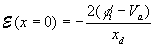
The electric field varies linearly in the depletion region and reaches a maximum value at x = 0 as can be seen on Figure 4.3.1(b). This maximum field can be calculated on either side of the depletion region, yielding: |
 | (4.3.11) |
This provides the first relationship between the two unknowns, xp and xn, namely: |
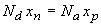 | (4.3.12) |
This equation expresses the fact that the total positive charge in the n-type depletion region, Qn, exactly balances the total negative charge in the p-type depletion region, Qp. We can then combine equation (4.3.4) with expression (4.3.12) for the total depletion-layer width, xd, yielding: |
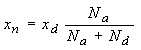 | (4.3.13) |
and |
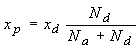 | (4.3.14) |
The potential in the semiconductor is obtained from the electric field using: |
 | (4.3.15) |
We therefore integrate the electric field yielding a piece-wise parabolic potential versus position as shown in Figure 4.3.1 (c) |
The total potential across the semiconductor must equal the difference between the built-in potential and the applied voltage, which provides a second relation between xp and xn, namely: |
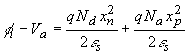 | (4.3.16) |
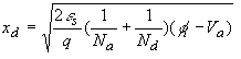
The depletion layer width is obtained by substituting the expressions for xp and xn, (4.3.13) and (4.3.14), into the expression for the potential across the depletion region, yielding: |
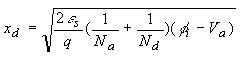 | (4.3.17) |
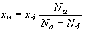
from which the solutions for the individual depletion layer widths, xp and xn are obtained: |
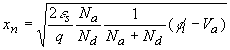 | (4.3.18) |
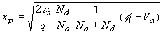 | (4.3.19) |
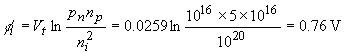
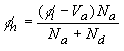
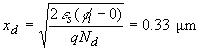
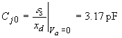
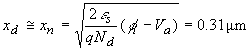
| Example 4.2 | An abrupt silicon (nI = 1010 cm-3) p-n junction consists of a p-type region containing 1016 cm-3 acceptors and an n-type region containing 5 x 1016 cm-3 donors.
|
| Solution | The built-in potential is calculated from:
The depletion layer width is obtained from:
the electric field from
and the potential across the n-type region equals
where
one can also show that:
This yields the following numeric values:
|
4.3.4. Junction capacitance | |
Any variation of the charge within a p-n diode with an applied voltage variation yields a capacitance, which must be added to the circuit model of a p-n diode. This capacitance related to the depletion layer charge in a p-n diode is called the junction capacitance. |
The capacitance versus applied voltage is by definition the change in charge for a change in applied voltage, or: |
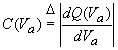 | (4.3.20) |
The absolute value sign is added in the definition so that either the positive or the negative charge can be used in the calculation, as they are equal in magnitude. Using equation (4.3.7) and (4.3.18) one obtains: |
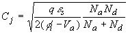 | (4.3.21) |
A comparison with equation (4.3.17), which provides the depletion layer width, xd, as a function of voltage, reveals that the expression for the junction capacitance, Cj, seems to be identical to that of a parallel plate capacitor, namely: |
 | (4.3.22) |
The difference, however, is that the depletion layer width and hence the capacitance is voltage dependent. The parallel plate expression still applies since charge is only added at the edge of the depletion regions. The distance between the added negative and positive charge equals the depletion layer width, xd. |
The capacitance of a p-n diode is frequently expressed as a function of the zero bias capacitance, Cj0: |
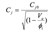 | (4.3.23) |
Where |
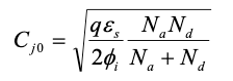 | (4.3.24) |
A capacitance versus voltage measurement can be used to obtain the built-in voltage and the doping density of a one-sided p-n diode. When plotting the inverse of the capacitance squared, one expects a linear dependence as expressed by: |
 | (4.3.25) |
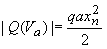
The capacitance-voltage characteristic and the corresponding 1/C2 curve are shown in Figure 4.3.2. |
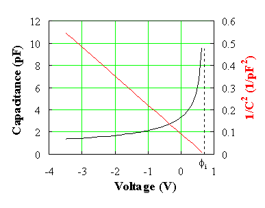 |
| Figure 4.3.2 : | Capacitance and 1/C2 versus voltage of a p-n diode with Na = 1016 cm-3, Nd = 1017 cm-3 and an area of 10-4 cm2. |
The built-in voltage is obtained at the intersection of the 1/C2 curve and the horizontal axis, while the doping density is obtained from the slope of the curve. |
 | (4.3.26) |
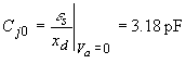
| Example 4.3 | Consider an abrupt p-n diode with Na = 1018 cm-3 and Nd = 1016 cm-3. Calculate the junction capacitance at zero bias. The diode area equals 10-4 cm2. Repeat the problem while treating the diode as a one-sided diode and calculate the relative error. |
| Solution | The built in potential of the diode equals:
The depletion layer width at zero bias equals:
And the junction capacitance at zero bias equals:
Repeating the analysis while treating the diode as a one-sided diode, one only has to consider the region with the lower doping density so that
And the junction capacitance at zero bias equals
The relative error equals 0.5 %, which justifies the use of the one-sided approximation.
|
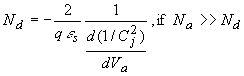
A capacitance-voltage measurement also provides the doping density profile of one-sided p-n diodes. For a p+-n diode, one obtains the doping density from: |
 | (4.3.27) |
while the depth equals the depletion layer width, obtained from xd = esA/Cj. Both the doping density and the corresponding depth can be obtained at each voltage, yielding a doping density profile. Note that the capacitance in equations (4.3.21), (4.3.22), (4.3.25), and (4.3.27) is a capacitance per unit area. |
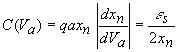
As an example, we consider the measured capacitance-voltage data obtained on a 6H-SiC p-n diode. The diode consists of a highly doped p-type region on a lightly doped n-type region on top of a highly doped n-type substrate. The measured capacitance as well as 1/C2is plotted as a function of the applied voltage. The dotted line forms a reasonable fit at voltages close to zero from which one can conclude that the doping density is almost constant close to the p-n interface. The capacitance becomes almost constant at large negative voltages, which corresponds according to equation (4.3.27) to a high doping density. |
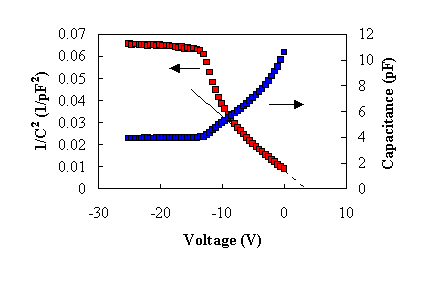 |
| Figure 4.3.3 : | Capacitance and 1/C2 versus voltage of a 6H-SiC p-n diode. |
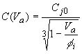
The doping profile calculated from the date presented in Figure 4.3.3 is shown in Figure 4.3.4. The figure confirms the presence of the highly doped substrate and yields the thickness of the n-type layer. No information is obtained at the interface (x = 0) as is typical for doping profiles obtained from C-V measurements. This is because the capacitance measurement is limited to small forward bias voltages since the forward bias current and the diffusion capacitance affect the accuracy of the capacitance measurement. |
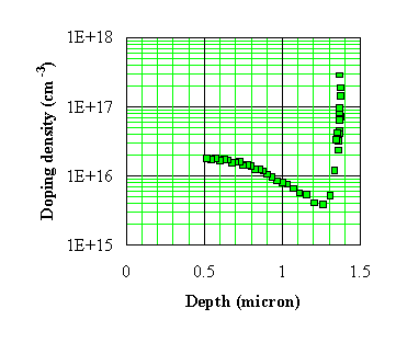 |
| Figure 4.3.4 : | Doping profile corresponding to the measured data, shown in Figure 4.3.3. |
4.3.5. The linearly graded p-n junction | |
A linearly graded junction has a doping profile, which depends linearly on the distance from the interface. |
 | (4.3.28) |
To analyze such junction we again use the full depletion approximation, namely we assume a depletion region with width xn in the n-type region and xp in the p-type region. Because of the symmetry, we can immediately conclude that both depletion regions must be the same. The potential across the junction is obtained by integrating the charge density between x = - xp and x = xn = xp twice resulting in: |
 | (4.3.29) |
Where the built-in potential is linked to the doping density at the edge of the depletion region such that: |
 | (4.3.30) |
The depletion layer with is then obtained by solving for the following equation: |
 | (4.3.31) |
Since the depletion layer width depends on the built-in potential, which in turn depends on the depletion layer width, this transcendental equation cannot be solved analytically. Instead it is solved numerically through iteration. One starts with an initial value for the built-in potential and then solves for the depletion layer width. A possible initial value for the built-in potential is the bandgap energy divided by the electronic charge, or 1.12 V in the case of silicon. From the depletion layer width, one calculates a more accurate value for the built-in potential and repeats the calculation of the depletion layer width. As one repeats this process, one finds that the values for the built-in potential and depletion layer width converge. |
The capacitance of a linearly graded junction is calculated like before as: |
 | (4.3.32) |
Where the charge per unit area must be recalculated for the linear junction, namely: |
 | (4.3.33) |
The capacitance then becomes: |
 | (4.3.34) |
The capacitance of a linearly graded junction can also be expressed as a function of the zero-bias capacitance or: |
 | (4.3.35) |
Where Cj0 is the capacitance at zero bias, which is given by: |
 | (4.3.36) |
Boulder, November 2007 |