4.7.1. P-i-N photodiodes


4.7.1. P-i-N photodiodes |      |
P-i-N photodiodes are commonly used in a variety of applications. A typical P-i-N photodiode is shown in Figure 4.7.1. It consists of a highly-doped transparent p-type contact layer on top of an undoped absorbing layer and an n-type highly doped contact layer on the bottom. Discrete photodiodes are fabricated on a conductive substrate as shown in the figure, which facilitates the formation of the n-type contact and reduces the number of process steps. The top contact is typically a metal ring contact, which has a low contact resistance and still allows the light to be absorbed in the semiconductor. An alternative approach uses a transparent conductor such as Indium Tin Oxide (ITO). The active device area is formed by mesa etching or by proton implantation of the adjacent area, which makes it isolating. A dielectric layer is added around the active area to reduce leakage currents and to ensure a low parasitic capacitance of the contact pad. |
 |
| Figure 4.7.1 : | Top view and vertical structure through section A-A' of a P-i-N heterostructure photodiode. |
Grading of the material composition between the transparent contact layer and the absorbing layer is commonly used to reduce the n-n+ or p-p+ barrier formed at the interface. |
However, the collection of carriers due to diffusion is relatively inefficient and leads to long tails in the transient response. It therefore should be avoided. |
 | 0 |
For instance, the reflection between air and GaAs (n = 3.5) is 31 %. |
The reflectivity for an arbitrary incident angle is: |
 | (4.7.2) |
 | (4.7.3) |
with |
where qi is the incident angle, and qt the transmitted angle. RTE is the reflectivity if the electric field is parallel to the surface while RTM is the reflectivity if the magnetic field is parallel to the surface. The reflectivity as a function of qi, for an air-GaAs interface is shown in Figure 4.7.2: |
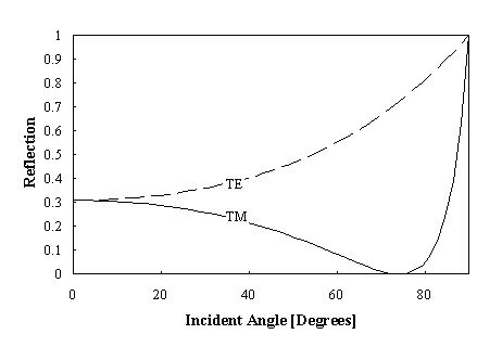 |
| Figure 4.7.2 : | Reflectivity versus incident angle for a transverse electric, RTE, and transverse magnetic, RTM, incident field. |
The generation of electron-hole pairs in a semiconductor is directly related to the absorption of light since every absorbed photon generates one electron-hole pair. The optical generation rate gop is given by: |
 | (4.7.4) |
where A is the illuminated area of the photodiode, Popt is the incident optical power, a is the absorption coefficient and hn is the photon energy. Note that the optical power is position dependent and obtained by solving: |
 | (4.7.5) |
The resulting generation rate must be added to the continuity equation and solved throughout the photodiode, which results in the photocurrent. |
Assuming that all the generated electron-hole pairs contribute to the photocurrent, the photocurrent is simply the integral of the generation rate over the depletion region: |
 | (4.7.6) |
where d is the thickness of the undoped region. The minus sign is due to the sign convention indicated on Figure 4.7.1. For a P-i-N diode with heavily doped n-type and p-type regions and a transparent top contact layer, this integral reduces to: |
 | (4.7.7) |
where Pin is the incident optical power and R is the reflection at the surface. |
To find the photocurrent due to absorption in the quasi-neutral region, we first have to solve the diffusion equation in the presence of light. For holes in the n-type contact layer this means solving the continuity equation: |
 | (4.7.8) |
Where the electron-hole pair generation gop depends on position. For an the n-type contact layer with the same energy bandgap as the absorption layer, the optical generation rate equals: |
 | (4.7.9) |
and the photocurrent due to holes originating in the n-type contact layer equals: |
 | (4.7.10) |
The first term is due to light whereas the second term is the due to thermal generation of electron-hole pairs. This derivation assumes that the thickness of the n-type contact layer is much larger than the diffusion length. |
Even though the contact layer was designed so that no light absorbs in this layer, it will become absorbing at shorter wavelengths. Consider a worst-case scenario where all the electron-hole pairs, which are generated in the p-type contact layer, recombine without contributing to the photocurrent. The optical power incident on the undoped region is reduced by exp(-a*wp�) where wp� is the width of the quasi-neutral p region and a* is the absorption coefficient in that region. |
Combining all the above effects the total responsivity of the detector - ignoring the dark current - equals: |
 | (4.7.11) |
Note that a*, a and hn are wavelength dependent. For a direct bandgap semiconductor these are calculated from: |
 | (4.7.12) |
The quantum efficiency then equals: |
 | (4.7.13) |
The dark current of a p-n diode including the ideal diode current, as well as recombination/generation in the depletion region is given by: |
 | (4.7.14) |
Under reverse bias conditions this expression reduces to: |
 | (4.7.15) |
The ideal diode current due to recombination of electrons has been ignored since np0 = ni,p2/Na is much smaller than pn0 because the p-layer has a larger band gap. In the undoped region, one expects the trap-assisted generation to be much larger than bimolecular generation. Which further reduces the current to: |
 | (4.7.16) |
The trap-assisted recombination tends to dominate for most practical diodes. |
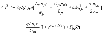
Noise in a p-i-n photodiode is primarily due to shot noise; the random nature of the generation of carriers in the photodiode yields also a random current fluctuation. The square of the current fluctuations equals: |
 | (4.7.17) |
where Ij are the currents due to different recombination/generation mechanisms and Df is the frequency range. Including the ideal diode current, Shockley-Hall-Read and band-to-band recombination as well as generation due to light one obtains: |
 | (4.7.18) |
The minimum detectable input power depends on the actual signal and the required signal to noise ration. As a first approximation, we now calculate the minimum detectable power as the power, which generates a current equal to the RMS noise current. A more detailed model for sinusoidal modulated signals is described in section 4.7.1.2.4. |
 | (4.7.19) |
The minimal noise current is obtained at Va = 0 for which the noise current and minimal power equal: |
 | (4.7.20) |
 | (4.7.21) |
The following derivation illustrates that shot noise and Johnson noise are not two independent noise mechanisms. In fact, we will show that both are the same for the special case of an ideal p-n diode under zero bias. At zero bias the photodetector can also be modeled as a resistor. Therefore the expression for Johnson noise should apply: |
 | (4.7.22) |
The resistance of a photodiode with |
 | (4.7.23) |
or for zero bias, the Johnson noise current is given by: |
 | (4.7.24) |
whereas the shot noise current at Va = 0 is given by: |
 | (4.7.25) |
where we added the noise due to the diffusion current to the noise due to the (constant) drift current, since both noise mechanisms do not cancel each other. Equations (4.7.24) and (4.7.25) are identical, thereby proving the equivalence between shot noise and Johnson noise in a photodiode at zero voltage. Note that this relation does not apply if the current is dominated by trap-assisted recombination/generation in the depletion region because of the non-equilibrium nature of the recombination/generation process. |
For a diode current of 1mA, a bandwidth Df of 1 GHz and a responsivity, R, of 0.2A/W, the noise current |
If the diode current is only due to the optical power, or I = PminR, then |
 | (4.7.26) |
The sensitivity for a given bandwidth can also be expressed as a number of photons per bit: |
 | (4.7.27) |
For instance, for a minimal power of -30 dBm and a bandwidth of 1 GHz, this sensitivity corresponds to 4400 photons per bit. |
Assume the optical power with average value P0 is amplitude modulated with modulation depth, m, as described by: |
 | (4.7.28) |
The ac current (RMS value) in the photodiode with responsivity, R, is then |
 | (4.7.29) |
which yields as an equivalent circuit of the photodiode a current source |
 | (4.7.30) |
where the equivalent dark current also includes the Johnson noise of the resistor, Req: |
 | (4.7.31) |
The signal to noise ratio is then given by: |
 | (4.7.32) |
from the above equation one can find the required optical power P0 needed to obtain a given signal to noise ratio, S/N: |
 | (4.7.33) |
The noise equivalent power is now defined as the ac (RMS) optical power needed to obtain a signal-to-noise ratio of one for a bandwidth of 1 Hz or: |
 | (4.7.34) |
We now consider two limiting case in which the NEP is either limited by the optical power or by the dark current. |
For |
 | (4.7.35) |
The noise equivalent power can also be used to calculate the ac optical power if the bandwidth differs from 1Hz from: |
 | (4.7.36) |
where the noise equivalent power has units of W/Hz. However, the optical power is mostly limited by the dark current for which the expressions are derived below. |
For |
 | (4.7.37) |
Again one can use the noise equivalent power to calculate the minimum detectable power for a given bandwidth: |
 | (4.7.38) |
where the noise equivalent power has now units of |
A rigorous solution for the switching time of a P-i-n photodiode starts from the continuity equations for electrons and holes: |
 | (4.7.39) |
 | (4.7.40) |
with |
 | (4.7.41) |
 | (4.7.42) |
and the electric field is obtained from Gauss's law. For a P-i-n diode with generation only at t = 0 and neglecting recombination and diffusion these equations reduce to: |
 | (4.7.43) |
Where the electric field, |
 | (4.7.44) |
replacing n(x,t) by n*(x - vnt) and p(x,t) by p*(x - vpt) yields vn = -mn |
The carrier distributions therefore equal those at t = 0 but displaced by a distance mn |
 | (4.7.45) |
 | (4.7.46) |
 | (4.7.47) |
for t < |d/vn| and t < |d/vp| . For a uniform carrier generation this reduces to: |
 | (4.7.48) |
 | (4.7.49) |
In the special case where vn = vp or mn = mp, the full width half maximum (FWHM) of the impulse response is: |
 | (4.7.50) |
Note: Rule of thumb to convert a pulse response to �3 dB frequency: |
 | (4.7.51) |
Since the bandwidth depends on the transit time, which in turn depends on the depletion layer width, there is a tradeoff between the bandwidth and the quantum efficiency. |
If we simplify the SHR recombination rate to n/t and p/t and assume a constant electric field and initial condition n(x,0) = n0 , the electron concentration can be obtained by solving the continuity equation, yielding: |
 | (4.7.52) |
where |
 | (4.7.53) |
with |
 | (4.7.54) |
For this analysis we solved the continuity equation with n(0,t) = n(L,t) = 0 implying infinite recombination at the edges of the depletion region. The initial carrier concentration n0 can also be related to the total energy which is absorbed in the diode at time t = 0: |
 | (4.7.55) |
and the photo current (calculated as described above) is |
 | (4.7.56) |
with Ck given by |
 | (4.7.57) |
The above equations can be used to calculate the impulse response of a photodiode. Each equation must be applied to electrons as well as holes since both are generated within the diode. Typically electrons and holes have a different mobility, which results in two regions with different slopes. This effect is clearly visible in GaAs diodes as illustrated with the figure below. |
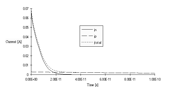 |
| Figure 4.7.3 : | Photocurrent calculated using equation (5.1.50) for a GaAs diode with fI -Va = 0.3 V, Epulse = 10-13 J, Eph = 2 eV and d = 2mm. |
Whereas section 4.7.1.3.1 provides a solution to the pulse response, one can also solve the frequency response when illuminating with a photon flux F1ejwt. If the photodiode has a linear response, both methods should be equivalent. To simplify the derivation, we assume that the total flux (in photons/s cm2) is absorbed at x = 0. This is for instance the case for a p-i-n diode with a quantum well at the interface between the p-type and intrinsic region and which is illuminated with long wavelength photons, which only absorb in the quantum well. The carriers moving through the depletion region cause a conduction current, Jcond(x): |
 | (4.7.58) |
where vn = mn |
From Ampere's law applied to a homogeneous medium, we find: |
 | (4.7.59) |
And the total current is the sum of the conduction and the displacement current: |
 | (4.7.60) |
If we assume that the electric field is independent of time, the total photo current equals |
 | (4.7.61) |
with transit time |
 | (4.7.62) |
For an infinitely long quasi-neutral (Q.N.) region and under stationary conditions, the generated carriers are only collected if they are generated within a diffusion length of the depletion region. The average time to diffuse over one diffusion length is the recombination time, t. Postulating a simple exponential time response we find that the current equals |
 | (4.7.63) |
Because of the relatively long carrier lifetime in fast photodiodes, carriers absorbed in the quasi-neutral region produce a long "tail" in the pulse response and should be avoided. |
The dynamic range is the ratio of the maximal optical power which can be detected to the minimal optical power. In most applications the dynamic range implies that the response is linear as well. The saturation current, defined as the maximum current which can flow through the external circuit, equals: |
 | (4.7.64) |
which yields an optimistic upper limit for the optical power: |
 | (4.7.65) |
and the dynamic range is defined as the ratio of the maximum to the minimum power: |
 | (4.7.66) |
Using (4.7.19) for the minimum power the dynamic range becomes independent of the responsivity and equals: |
 | (4.7.67) |
For example, if the equivalent noise current equals Ieq = 1mA, the bandwidth Df = 1 GHz, the impedance R = 50 W, and the applied voltage Va = 0, then the dynamic range equals 1.35 x 10⁶ (for fi = 1.2 V) or 61.3 dB. |
4.7.2. Photoconductors |      |
Photoconductors consist of a piece of semiconductor with two Ohmic contacts. Under illumination, the conductance of the semiconductor changes with the intensity of the incident optical power. The current is mainly due to majority carriers since they are free to flow across the Ohmic contacts. However the majority carrier current depends on the presence of the minority carriers. The minority carriers pile up at one of the contacts, where they cause additional injection of majority carriers until the minority carriers recombine. This effect can cause large "photoconductive" gain, which depends primarily of the ratio of the minority carrier lifetime to the majority carrier transit time. Long carrier lifetimes therefore cause large gain, but also a slow response time. The gain-bandwidth product of the photoconductor is almost independent of the minority carrier lifetime and depends only on the majority carrier transit time. |
Consider now a photoconductor with length, L, width W and thickness d, which is illuminated a total power, P. The optical power, P(x), in the material decreases with distance due to absorption and is described by: |
 | (4.7.68) |
The optical power causes a generation of electrons and holes in the material. Solving the diffusion equation (4.7.8) for the steady state case and in the absence of a current density gradient one obtains for the excess carrier densities: |
 | (4.7.69) |
Where it was assumed that the majority carriers, which primarily contribute to the photocurrent, are injected from the contacts as long as the minority carriers are present. The photo current due to the majority carriers (here assumed to be n-type) is: |
 | (4.7.70) |
where tr is the majority carrier transit time given by: |
 | (4.7.71) |
The equation above also includes the power reduction due to the reflection at the surface of the semiconductor. The normalized photocurrent is plotted in Figure 4.7.4 as a function of the normalized layer thickness for different ratio of lifetime to transit time. |
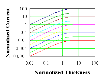 |
| Figure 4.7.4: | Normalized current  versus normalized thickness ad as a function of the ratio of the minority carrier lifetime to the majority carrier transit time, t/tr, ranging from 0.01 (bottom curve) to 100 (top curve) versus normalized thickness ad as a function of the ratio of the minority carrier lifetime to the majority carrier transit time, t/tr, ranging from 0.01 (bottom curve) to 100 (top curve) |
As an example, consider a silicon photoconductor with mn = 1400 cm2/V-s and t = 1 ms. The photoconductor has a length of 10 micron and width of 100 micron. For an applied voltage of 5 Volt, the transit time is 143 ps yielding a photoconductive gain of 7000. For a normalized distance ad = 1 and incident power of 1 mW the photocurrent equals 1.548 mA. A reflectivity of 30 % was assumed at the air/silicon interface. |
High photoconductive gain is typically obtained for materials with a long minority carrier lifetime, t, high mobility, mn, and above all a photoconductor with a short distance, L, between the electrodes. |
4.7.3. Metal-Semiconductor-Metal (MSM) Photodetectors |      |
Metal-semiconductor-metal photodetectors are the simplest type of photodetectors since they can be fabricated with a single mask. They typically consist of a set of interdigitated fingers, resulting in a large active area and short distance between the electrodes. |
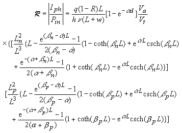
The responsivity for a detector with thickness, d, surface reflectivity, R, finger spacing, L, and finger width, w, is given by: |
 | (4.7.72) |
Where a is the absorption length and the reflectivity, R, of the air-semiconductor interface as a function of the incident angle is given by: |
 | (4.7.73) |
 | (4.7.74) |
with |
with qi the incident angle, and qt the transmitted angle. RTE is the reflectivity if the electric field is parallel to the surface while RTM is the reflectivity if the magnetic field is parallel to the surface. The reflectivity as a function of qi, for an air-GaAs interface is shown in Figure 4.7.5: |
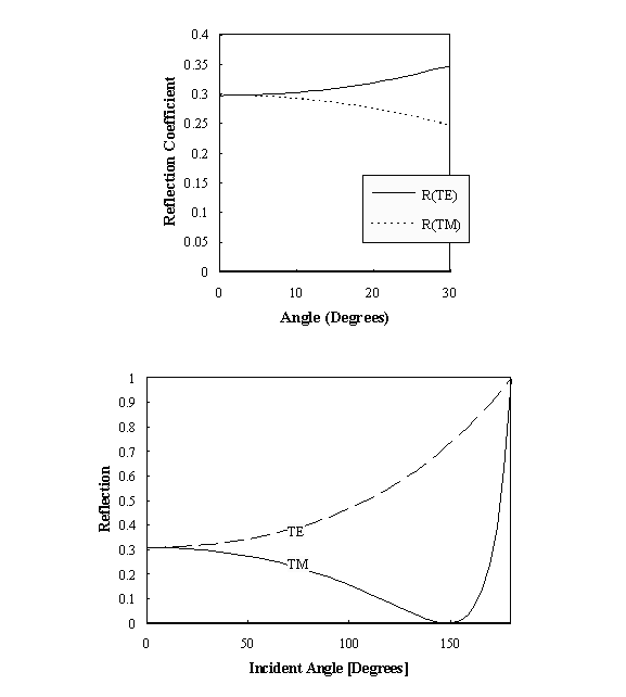 |
| Figure 4.7.5: | Angular dependencies of the reflectivity of an Air-to-GaAs interface |
Including drift, diffusion and recombination the responsivity becomes: |
 | (4.7.75) |
with |
 | (4.7.80) |
The above expression can be used to calculate the current as a function of the applied voltage. An example is shown in Figure 4.7.6. Both the electron and the hole current are plotted as is the total current. The difference between the electron and hole current is due to the recombination of carriers. For large voltages all photo-generated carriers are swept out yielding a saturation of the photocurrent with applied voltage, whereas for small voltages around zero diffusion is found to be the dominant mechanism. The ratio of the transit time to the diffusion time determines the current around zero volt. In the absence of velocity saturation both transit times depend on the carrier mobility so that the ratio becomes independent of the carrier mobility. This causes the I-V curves to be identical for electrons and holes in the absence of recombination. |
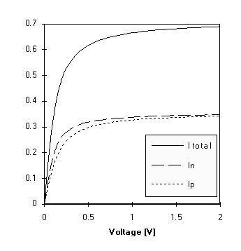 |
| Figure 4.7.6: | Current - Voltage characteristic of an MSM photodiode. |
The pulse response can be calculated by solving the time dependent continuity equation, yielding: |
 | (4.7.81) |
with Ck given by: |
 | (4.7.82) |
where |
 | (4.7.83) |
and |
 | (4.7.84) |
This solution is plotted in Figure 4.7.7. |
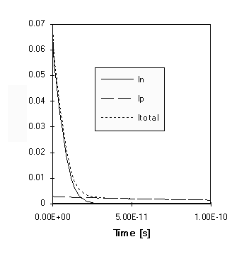 |
| Figure 4.7.7: | Transient behavior (Pulse energy, Epulse = 0.1 pJ, Va = 0.3V) |
The equivalent circuit of the diode consists of the diode capacitance, Cp, a parallel resistance, Rp, obtained from the slope of the I-V characteristics at the operating voltage in parallel to the photocurrent, Iph, which is obtained by calculating the convolution of the impulse response and the optical input signal. A parasitic series inductance, LB, primarily due to the bond wire, and a series resistance, Rs, are added to complete the equivalent circuit shown in Figure 4.7.8. |
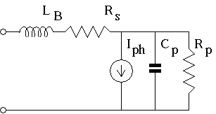 |
| Figure 4.7.8: | Equivalent circuit of an MSM detector |