
The MOS capacitor consists of a Metal-Oxide-Semiconductor structure as illustrated by Figure 6.2.1. Shown is the semiconductor substrate with a thin oxide layer and a top metal contact, referred to as the gate. A second metal layer forms an Ohmic contact to the back of the semiconductor and is called the bulk contact. The structure shown has a p-type substrate. We will refer to this as an n-type MOS or nMOS capacitor since the inversion layer - as discussed in section 6.6.4 - contains electrons. |
 |
| Figure 6.2.1: | MOS capacitance structure |
To understand the different bias modes of an MOS capacitor we now consider three different bias voltages. One below the flatband voltage, VFB, a second between the flatband voltage and the threshold voltage, VT, and finally one larger than the threshold voltage. These bias regimes are called the accumulation, depletion and inversion mode of operation. These three modes as well as the charge distributions associated with each of them are shown in Figure 6.2.2. |
 |
| Figure 6.2.2.: | Charges in an n-type Metal-Oxide-Semiconductor structure (p-type substrate) under accumulation, depletion and inversion conditions. |
Accumulation occurs typically for negative voltages where the negative charge on the gate attracts holes from the substrate to the oxide-semiconductor interface. Depletion occurs for positive voltages. The positive charge on the gate pushes the mobile holes into the substrate. Therefore, the semiconductor is depleted of mobile carriers at the interface and a negative charge, due to the ionized acceptor ions, is left in the space charge region. The voltage separating the accumulation and depletion regime is referred to as the flatband voltage, VFB. Inversion occurs at voltages beyond the threshold voltage. In inversion, there exists a negatively charged inversion layer at the oxide-semiconductor interface in addition to the depletion-layer. This inversion layer is due to the minority carriers that are attracted to the interface by the positive gate voltage. |
The energy band diagram of an n-MOS capacitor biased in inversion is shown in Figure 6.2.3. The oxide is modeled as a semiconductor with a very large bandgap and blocks any flow of carriers between the semiconductor and the gate metal. The band bending in the semiconductor is consistent with the presence of a depletion layer. At the semiconductor-oxide interface, the Fermi energy is close to the conduction band edge as expected when a high density of electrons is present. The semiconductor remains in thermal equilibrium even when a voltage is applied to the gate. The presence of an electric field does not automatically lead to a non-equilibrium condition, as was also the case for a p-n diode with zero bias. |
 |
| Figure 6.2.3: | Energy band diagram of an MOS structure biased in inversion. |
In the next sections, we discuss the four modes of operation of an MOS structure: Flatband, Depletion, Inversion and Accumulation. Flatband conditions exist when no charge is present in the semiconductor so that the silicon energy band is flat. Initially we will assume that this occurs at zero gate bias. Later we will consider the actual flatband voltage in more detail. Surface depletion occurs when the holes in the substrate are pushed away by a positive gate voltage. A more positive voltage also attracts electrons (the minority carriers) to the surface, which form the so-called inversion layer. Under negative gate bias, one attracts holes from the p-type substrate to the surface, yielding accumulation. |
6.2.1. Flatband diagram |      |
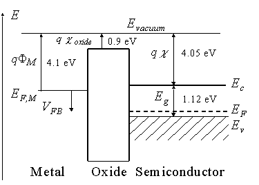
The flatband diagram is by far the easiest energy band diagram. The term flatband refers to fact that the energy band diagram of the semiconductor is flat, which implies that no charge exists in the semiconductor. The flatband diagram of an aluminum-silicon dioxide-silicon MOS structure is shown in Figure 6.2.4. Note that a voltage, VFB, must be applied to obtain this flat band diagram. Indicated on the figure is also the work function of the aluminum gate, FM, the electron affinity of the oxide, coxide, and that of silicon, c, as well as the bandgap energy of silicon, Eg. The bandgap energy of the oxide is quoted in the literature to be between 8 and 9 electron volt. The reader should also realize that the oxide is an amorphous material and the use of semiconductor parameters for such material can justifiably be questioned. |
The flatband voltage is obtained when the applied gate voltage equals the workfunction difference between the gate metal and the semiconductor. If there is a fixed charge in the oxide and/or at the oxide-silicon interface, the expression for the flatband voltage must be modified accordingly. |
 |
| Figure 6.2.4: | Flatband energy diagram of a metal-oxide-semiconductor (MOS) structure consisting of an aluminum metal, silicon dioxide and silicon. |
6.2.2. Accumulation |      |
Accumulation occurs when one applies a voltage less than the flatband voltage. The negative charge on the gate attracts holes from the substrate to the oxide-semiconductor interface. Only a small amount of band bending is needed to build up the accumulation charge so that almost all of the potential variation is within the oxide. |
6.2.3. Depletion |      |
As a more positive voltage than the flatband voltage is applied, a negative charge builds up in the semiconductor. Initially this charge is due to the depletion of the semiconductor starting from the oxide-semiconductor interface. The depletion layer width further increases with increasing gate voltage. |
6.2.4. Inversion |      |
As the potential across the semiconductor increases beyond twice the bulk potential, another type of negative charge emerges at the oxide-semiconductor interface: this charge is due to minority carriers, which form a so-called inversion layer. As one further increases the gate voltage, the depletion layer width barely increases further since the charge in the inversion layer increases exponentially with the surface potential. |