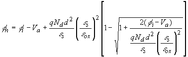
A more elaborate model of the Schottky barrier contains an interfacial layer between the semiconductor and the metal. Typically this layer is a thin oxide layer, with thickness d, which naturally forms on the surface of a semiconductor when exposed to air. The analysis of the Schottky diode can now be repeated using the full depletion approximation yielding the following relation between the total applied voltage and the depletion layer width: |
 | (3.7.1) |
from which the depletion layer width can be solved. The capacitance of the structure can be obtained from the series connection of the oxide and semiconductor capacitance: |
 | (3.7.2) |
with |
 | (3.7.3) |
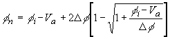
This expression is very similar to that of equation (3.3.10) except that the oxide layer increases the built-in voltage. The potential fn across the semiconductor can be written as: |
 | (3.7.4) |
Or alternatively, |
 | (3.7.5) |
for zero applied voltage this reduces to: |
 | (3.7.6) |
instead of simply fn = fi when no oxide is present. This analysis can be interpreted as follows: the interfacial layer reduces the capacitance of the Schottky barrier diode, although a capacitance measurement will have the same general characteristics as an ideal Schottky barrier diode except that the built-in voltage is increased. However the potential across the semiconductor is decreased due to the voltage drop across the oxide layer, so that at low voltage the barrier for electrons flowing into the semiconductor is reduced yielding a higher current that without the oxide. This analysis assumes that the interfacial layer forms a very thin tunnel barrier, which at low voltages does not restrict the current. As the voltage applied to the Schottky barrier is more positive, the depletion layer width reduces, so that the field in the oxide also reduces and with it the voltage drop across the oxide. The current under forward bias conditions therefore approaches that of the ideal Schottky diode until the tunnel barrier restricts the current flow. This results in a higher ideality factor for Schottky barrier with an interfacial layer. From equations (3.7.3) and (3.7.4) we find that the effect is largest for highly doped semiconductors and interfacial layers with low dielectric constant. |
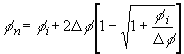
The current under forward bias is then given by: |
 | (3.7.7) |
or: |
 | (3.7.8) |
which, around a specific value of Va , can be written as: |
 | (3.7.9) |
with ideality, n: |
 | (3.7.10) |
and saturation current Is*: |
 | (3.7.11) |
At Va = 0 the saturation current becomes: |
 | (3.7.12) |
As a result, an interfacial layer between the metal and semiconductor of a Schottky diode affects both the measured barrier height and built-in potential. The total potential within the device is now divided between the interfacial layer and the semiconductor. This causes the potential across the semiconductor to be lower so that carriers can more easily flow from the semiconductor into the metal, yielding a larger current. The interfacial layer also reduces the capacitance. |
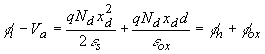
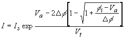
As an example we consider a thin 3 nm thick oxide layer at the interface of a gold-silicon Schottky diode. The energy band diagram is shown in Figure 3.7.1. |
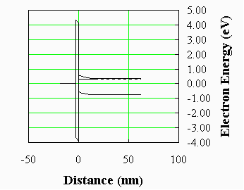 |
| Figure 3.7.1: | Energy band diagram of a gold-silicon M-S junction with a 3 nm interfacial oxide layer. (Va = 0.3 V and Nd = 1018 cm-3) |
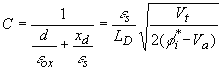
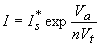
Since the interfacial layer can be viewed as an additional capacitor connected in series with the capacitance associated with the depletion layer, the total capacitance is lower than for a diode without an interfacial layer. A 1/C2 plot versus the applied voltage is shown in Figure 3.7.2. |
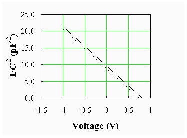 |
| Figure 3.7.2: | Capacitance-Voltage characteristics of a gold-silicon M-S junction with (solid line) and without (dashed line) a 3 nm interfacial oxide layer. (Nd = 1018 cm-3) |
This plot reveals that the slope remains the same, while the intercept with the voltage axis shifts to higher forward voltages. The slope remains unchanged since it depends on the doping concentration in the semiconductor, which remains unchanged. The presence of an interfacial layer therefore increases the measured built-in potential, but does not alter the extracted doping concentration. |
The analysis of the forward bias current is more complex since it depends on the transport properties of the interfacial layer. However, if one assumes that the barrier is so thin that carriers can easily tunnel through, the diode current analysis can be obtained from the standard diffusion analysis, provided that the altered potential across the semiconductor is taken into account. |
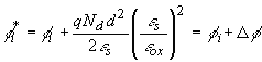
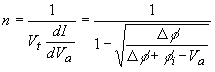
A comparison of the current through a gold-silicon junction with and without an interfacial layer is shown in Figure 3.7.3. The figure reveals that the interfacial layer affects both the slope and the intercept of the forward-biased current-voltage when plotted on a semi-logarithmic scale. |
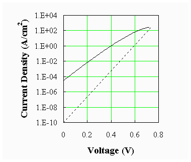 |
| Figure 3.7.3: | Current-Voltage characteristics of a gold-silicon M-S junction with (solid line) and without (dashed line) a 3 nm interfacial oxide layer. (Is = 10-10 A and Nd = 1018 cm-3) |
In summary, an interfacial layer increases the built-in potential as measured with a C-V measurement, decreases the internal potential across the semiconductor, which increases the measured ideality factor and saturation current. It also decreases the measured barrier height as extracted from the temperature dependence of the saturation current and limits the maximum current density. |