
 2.3.8. Derivation of the Kronig-Penney equation
2.3.9. Alternate derivation of the Kronig-Penney equation
2.3.8. Derivation of the Kronig-Penney equation
2.3.9. Alternate derivation of the Kronig-Penney equation
Energy bands consisting of a large number of closely spaced energy levels exist in crystalline materials. The bands can be thought of as the collection of the individual energy levels of electrons surrounding each atom. The wavefunctions of the individual electrons, however, overlap with those of electrons confined to neighboring atoms. The Pauli exclusion principle does not allow the electron energy levels to be the same so that one obtains a set of closely spaced energy levels, forming an energy band. The energy band model is crucial to any detailed treatment of semiconductor devices. It provides the framework needed to understand the concept of an energy bandgap and that of conduction in an almost filled band as described by the empty states. |
In this section, we present the free electron model and the Kronig-Penney model. Then we discuss the energy bands of semiconductors and present a simplified band diagram. We also introduce the concept of holes and the effective mass. |
2.3.1 Free electron model |   |
The free electron model of metals has been used to explain the photo-electric effect (see section 1.2.2). This model assumes that electrons are free to move within the metal but are confined to the metal by potential barriers as illustrated by Figure 2.3.1. The minimum energy needed to extract an electron from the metal equals qFM, where FM is the workfunction. This model is frequently used when analyzing metals. However, this model does not work well for semiconductors since the effect of the periodic potential due to the atoms in the crystal has been ignored. |
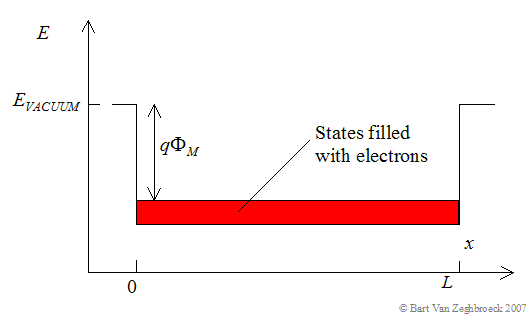 |
| Figure 2.3.1.: | The free electron model of a metal. |
2.3.2 Periodic potentials | |
The analysis of periodic potentials is required to find the energy levels in a semiconductor. This requires the use of periodic wave functions, called Bloch functions which are beyond the scope of this text. The result of this analysis is that the energy levels are grouped in bands, separated by energy band gaps. The behavior of electrons at the bottom of such a band is similar to that of a free electron. However, the electrons are affected by the presence of the periodic potential. The combined effect of the periodic potential is included by adjusting the value of the electron mass. This mass will be referred to as the effective mass. |
The effect of a periodic arrangement on the electron energy levels is illustrated by Figure 2.3.2. Shown are the energy levels of electrons in a carbon crystal with the atoms arranged in a diamond lattice. These energy levels are plotted as a function of the lattice constant, a. |
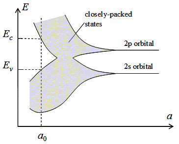 |
| Figure 2.3.2. : | Energy bands for diamond versus lattice constant. |
Isolated carbon atoms contain six electrons, which occupy the 1s, 2s and 2p orbital in pairs. The energy of an electron occupying the 2s and 2p orbital is indicated on the figure. The energy of the 1s orbital is not shown. As the lattice constant is reduced, there is an overlap of the electron wavefunctions occupying adjacent atoms. This leads to a splitting of the energy levels consistent with the Pauli exclusion principle. The splitting results in an energy band containing 2N states in the 2s band and 6N states in the 2p band, where N is the number of atoms in the crystal. A further reduction of the lattice constant causes the 2s and 2p energy bands to merge and split again into two bands containing 4N states each. At zero Kelvin, the lower band is completely filled with electrons and labeled as the valence band. The upper band is empty and labeled as the conduction band. |
The Kronig-Penney model demonstrates that a simple one-dimensional periodic potential yields energy bands as well as energy band gaps. While it is an oversimplification of the three-dimensional potential and bandstructure in an actual semiconductor crystal, it is an instructive tool to demonstrate how the band structure can be calculated for a periodic potential, and how allowed and forbidden energies are obtained when solving the corresponding Schrödinger equation. |
The potential assumed in the model is shown in the Figure 2.3.3: |
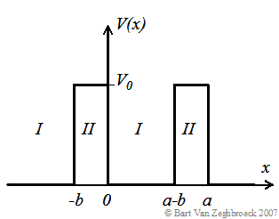 |
| Figure 2.3.3 : | The periodic potential assumed in the Kronig-Penney model. The potential barriers (region I) with width, b, are spaced by a distance (region II), a-b, and repeated with a period, a. |
The Kronig-Penney consists of an infinite series of rectangular barriers with potential height, V0, and width, b, separated by a distance, a-b, resulting in a periodic potential with period, a. The analysis requires the use of Bloch functions, traveling wave solutions multiplied with a periodic function, which has the same periodicity as the potential. The actual derivation can be found in section 2.3.8. |
Solutions for k and E are obtained when the following equation is satisfied: |
 | (2.3.1) |
where |
 | (2.3.2) |
This transcendental equation can be further simplified for the case where the barrier is a delta function with area, V0b, for which it becomes: |
 | (2.3.3) |
with |
 | (2.3.4) |
This equation can only be solved numerically. Solutions are only obtained if the function, F, is between -1 and 1 since it has to equal cos(ka). The energy, E, is plotted as function of ka/p and the function F in Figure 2.3.4. |
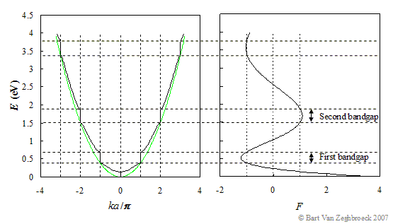 |
| Figure 2.3.4.: | Graphical solution to the Kronig-Penney model for a = 1nm and V0b = 0.2 nm-eV. Shown is the energy, E, versus ka/p and F, which has to equal cos(ka), from which one can identify the allowed energies. |
The corresponding band structure is shown below (black curve) as well as the energy for a free electron (gray curve). Three different forms are presented, namely the E(k) digram, the E(k diagram combined with the reduced-zone diagram as well as the reduced-zone diagram only. |
 |
| Figure 2.3.5.: | Energy versus ka/p as presented in Figure 2.3.4 (black curves) compared to that of a free electron (gray curves). Shown are: a) the E(k) diagram, b) the E(k) diagram combined with the reduced-zone diagram and c) the reduced-zone diagram only. |
From Figure 2.3.5.a we observe the following: The E(k) relation resembles a parabola except that only specific ranges of energies are valid solutions to Schrödinger's equation and therefore are allowed, while others are not. The range of energies for which there is no solution is referred to as an energy band gap. The transitions between allowed and forbidden energies occur at non-zero integer multiples of ka/π. These correspond to local minima and maxima of the E(k) relation. The reduced-zone diagram shown in Figure 2.3.5.c contains the first three bands and energy bandgaps. For instance the second energy bandgap occurs between 1.5 and 2 eV, between the band maximum of the second band and the band minimum of the third band. |
2.3.3 Energy bands of semiconductors | |
Complete energy band diagrams of semiconductors are very complex. However, most have features similar to that of the diamond crystal discussed in section 2.3.2. In this section, we first take a closer look at the energy band diagrams of common semiconductors. We then present a simple diagram containing only the most important features and discuss the temperature and doping dependence of the energy bandgap. |
The energy band diagrams of semiconductors are rather complex. The detailed energy band diagrams of germanium, silicon and gallium arsenide are shown in Figure 2.3.6. The energy is plotted as a function of the wavenumber, k, along the main crystallographic directions in the crystal, since the band diagram depends on the direction in the crystal. The energy band diagrams contain multiple completely-filled and completely-empty bands. In addition, there are multiple partially-filled band. |
 |
| Figure 2.3.6.: | Energy band diagram of (a) germanium, (b) silicon and (c) gallium arsenide. |
Fortunately, we can simplify the energy band diagram since only the electrons in the highest almost-filled band and the lowest almost-empty band dominate the behavior of the semiconductor. These bands are indicated on the figure by the + and - signs corresponding to the charge of the carriers in those bands. |
The energy band diagrams shown in the previous section are frequently simplified when analyzing semiconductor devices. Since the electronic properties of a semiconductor are dominated by the highest partially empty band and the lowest partially filled band, it is often sufficient to only consider those bands. This leads to a simplified energy band diagram for semiconductors as shown in Figure 2.3.7: |
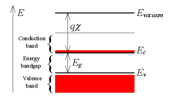 |
| Figure 2.3.7.: | A simplified energy band diagram used to describe semiconductors. Shown are the valence and conduction band as indicated by the valence band edge, Ev, and the conduction band edge, Ec. The vacuum level, Evacuum, and the electron affinity, c, are also indicated on the figure. |
The diagram identifies the almost-empty conduction band by a set of horizontal lines. The bottom line indicates the bottom edge of the conduction band and is labeled Ec. Similarly, the top of the valence band is indicated by a horizontal line labeled Ev. The energy band gap, Eg, is located between the two bands. The distance between the conduction band edge, Ec, and the energy of a free electron outside the crystal (called the vacuum level labeled Evacuum) is quantified by the electron affinity, χ multiplied with the electronic charge q. |
An important feature of an energy band diagram, which is not included on the simplified diagram, is whether the conduction band minimum and the valence band maximum occur at the same value for the wavenumber. If so, the energy bandgap is called direct. If not, the energy bandgap is called indirect. This distinction is of interest for optoelectronic devices since direct bandgap materials provide more efficient absorption and emission of light. More sppecifically, the smallest bandgap of germanium and silicon is indirect, while gallium arsenide has a direct bandgap as can be seen on Figure 2.3.6. |
The energy bandgap of semiconductors tends to decrease as the temperature is increased. This behavior can be understood if one considers that the interatomic spacing increases when the amplitude of the atomic vibrations increases due to the increased thermal energy. This effect is quantified by the linear expansion coefficient of a material. An increased interatomic spacing decreases the average potential seen by the electrons in the material, which in turn reduces the size of the energy bandgap. A direct modulation of the interatomic distance - such as by applying compressive (tensile) stress - also causes an increase (decrease) of the bandgap. |
The temperature dependence of the energy bandgap, Eg, has been experimentally determined yielding the following expression for Eg as a function of the temperature, T: |
 | (2.3.5) |
where Eg(0), α and β are the fitting parameters. These fitting parameters are listed for germanium, silicon and gallium arsenide in Table 2.3.1: |
 |
| Table 2.3.1.: | Parameters used to calculate the energy bandgap of germanium, silicon and gallium arsenide (GaAs) as a function of temperature. |
A plot of the resulting bandgap versus temperature is shown in Figure 2.3.8 for germanium, silicon and gallium arsenide. |
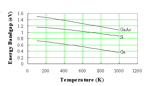 |
| Figure 2.3.8.: | Temperature dependence of the energy bandgap of germanium (Ge), silicon (Si) and gallium arsenide (GaAs).  |
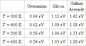
| Example 2.2 | Calculate the energy bandgap of germanium, silicon and gallium arsenide at 300, 400, 500 and 600 K. |
| Solution | The bandgap of silicon at 300 K equals:
Similarly one finds the energy bandgap for germanium and gallium arsenide, as well as at different temperatures, yielding:
|
High doping densities cause the bandgap to shrink. This effect is explained by the fact that the wavefunctions of the electrons bound to the impurity atoms start to overlap as the density of the impurities increase. For instance, at a doping density of 1018 cm-3, the average distance between two impurities is only 10 nm. This overlap forces the energies to split into an energy band rather than a discreet level. |
If the impurity level is shallow (see section 2.6.4.1), this impurity band reduces the energy band of the host material by |
 | (2.3.6) |
where N is the doping density, q is the electronic charge, εs is the dielectric constant of the semiconductor, k is Boltzmann's constant and T is the temperature in Kelvin. For silicon (εr = 11.9) this expression further reduces to: |
 | (2.3.7) |
From this expression we find that the bandgap shrinkage can typically be ignored for doping densities less than 1018 cm-3. |
A plot of the change in bandgap energy with doping density is shown in Figure 2.3.9: |
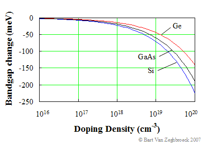 |
| Figure 2.3.9.: | Doping dependence of the energy bandgap of germanium (Ge), gallium arsenide (GaAs), and silicon (Si). |
2.3.4 Metals, insulators and semiconductors | |
Once we know the bandstructure of a given material we still need to find out which energy levels are occupied and whether specific bands are empty, partially filled or completely filled. |
Empty bands do not contain electrons. Therefore, they are not expected to contribute to the electrical conductivity of the material. Partially filled bands do contain electrons as well as available energy levels at slightly higher energies. These unoccupied energy levels enable carriers to gain energy when moving in an applied electric field. Electrons in a partially filled band therefore do contribute to the electrical conductivity of the material. |
Completely filled bands do contain plenty of electrons but do not contribute to the conductivity of the material. This is because the electrons cannot gain energy since all energy levels are already filled. |
In order to find the filled and empty bands we must find out how many electrons can be placed in each band and how many electrons are available. Each band is formed due to the splitting of one or more atomic energy levels. Therefore, the minimum number of states in a band equals twice the number of atoms in the material. The reason for the factor of two is that every energy level can contain two electrons with opposite spin. |
To further simplify the analysis, we assume that only the valence electrons (the electrons in the outer shell) are of interest. The core electrons are tightly bound to the atom and are not allowed to freely move in the material. |
Four different possible scenarios are shown in Figure 2.3.10: |
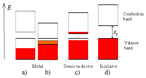 |
| Figure 2.3.10.: | Possible energy band diagrams of a crystal. Shown are: a) a half filled band, b) two overlapping bands, c) an almost full band separated by a small bandgap from an almost empty band and d) a full band and an empty band separated by a large bandgap. |
A half-filled band is shown in Figure 2.3.10 a). This situation occurs in materials consisting of atoms, which contain only one valence electron per atom. Most highly conducting metals including copper, gold and silver satisfy this condition. Materials consisting of atoms that contain two valence electrons can still be highly conducting if the resulting filled band overlaps with an empty band. This scenario is shown in b). No conduction is expected for scenario d) where a completely filled band is separated from the next higher empty band by a larger energy gap. Such materials behave as insulators. Finally, scenario c) depicts the situation in a semiconductor. The completely filled band is now close enough to the next higher empty band that electrons can make it into the next higher band. This yields an almost full band below an almost empty band. We will call the almost full band the valence band since it is occupied by valence electrons. The almost empty band will be called the conduction band, as electrons are free to move in this band and contribute to the conduction of the material. |
2.3.5 Electrons and holes in semiconductors | |
As pointed out in section 2.3.4, semiconductors differ from metals and insulators by the fact that they contain an "almost-empty" conduction band and an "almost-full" valence band. This also means that we will have to deal with the transport of carriers in both bands. |
To facilitate the discussion of the transport in the "almost-full" valence band of a semiconductor, we will introduce the concept of holes. It is important to understand that one could deal with only electrons if one is willing to keep track of all the electrons in the "almost-full" valence band. After all, electrons are the only real particles available in a semiconductor. |
The concepts of holes is introduced in semiconductors since it is easier to keep track of the missing electrons in an "almost-full" band, rather than keeping track of the actual electrons in that band. We will now first explain the concept of a hole and then point out how the hole concept simplifies the analysis. |
Holes are missing electrons. They behave as particles with the same properties as the electrons would have when occupying the same states except that they carry a positive charge. This definition is illustrated further with Figure 2.3.11, which presents the energy band diagram in the presence of an electric field. |
 |
| Figure 2.3.11.: | Energy band diagram in the presence of a uniform electric field. Shown are the upper almost-empty band and the lower almost-filled band. The tilt of the bands is caused by an externally applied electric field. |
A uniform electric field is assumed which causes a constant gradient of the bands, as described by:. |
 | (2.3.8) |
which is a modified form of Gauss' law, equation (1.3.5). |
The electrons in the almost-empty band are negatively charged particles, which therefore move in a direction, which opposes the direction of the field. Electrons therefore move down hill in the upper band. Electrons in the lower band also move in the same direction. The total current density due to the electrons in the valence band can therefore be written as: |
 | (2.3.9) |
where V is the volume of the semiconductor, q is the electronic charge and v is the electron velocity. The sum is taken over all occupied or filled states in the lower band. This equation can be reformulated by first taking the sum over all the states in the lower band and subtracting the current due to the electrons, which are missing in the almost-filled band. This last term therefore represents the sum taken over all the empty states in the lower band, or: |
 | (2.3.10) |
The sum over all the states in the lower band has to equal zero since electrons in a completely filled band do not contribute to current, while the remaining term can be written as: |
 | (2.3.11) |
which states that the current is due to positively charged particles associated with the empty states in the almost-filled band. We call these particles holes. Keep in mind that there is no real particle associated with a hole. Instead, the combined behavior of all the electrons, which occupy states in the almost-filled band, is the same as that of positively charge particles associated with the unoccupied states. |
The reason the concept of holes simplifies the analysis is that the density of states function of a whole band can be rather complex. However, it can be dramatically simplified if only states close to the band edge need to be considered. |
2.3.6 The effective mass concept | |
Electrons with an energy close to a band minimum behave as free electrons, since the E-k relation can be approximated by a parabola. They accelerate in an applied electric field just like a free electron in vacuum. Their wavefunctions are periodic and extend over the size of the material. The presence of the periodic potential, due to the atoms in the crystal without the valence electrons, changes the properties of the electrons. Therefore, the mass of the electron differs from the free electron mass, m0. Because of the anisotropy of the effective mass and the presence of multiple equivalent band minima, we define two types of effective mass: 1) the effective mass for density of states calculations and 2) the effective mass for conductivity calculations. The effective mass values for electrons and holes are listed together with the value of the smallest energy bandgap in Table 2.3.2. Electrons in gallium arsenide have an isotropic effective mass so that the conductivity effective mass equals the density of states effective mass. |
 |
| Table 2.3.2.: | Effective mass of carriers in germanium, silicon and gallium arsenide (GaAs) |
truenano.com/PSD20 | Boulder, January 2026 |

 :
: