4.10.1. Introduction |   |
Laser diodes consist of a p-n diode with an active region where electrons and holes recombine resulting in light emission. In addition, a laser diode contains an optical cavity where stimulated emission takes place. The laser cavity consists of a waveguide terminated on each end by a mirror. As an example, the structure of an edge-emitting laser diode is shown in Figure 4.10.1. Photons, which are emitted into the waveguide, can travel back and forth in this waveguide provided they are reflected at the mirrors. The distance between the two mirrors is the cavity length, labeled L. |
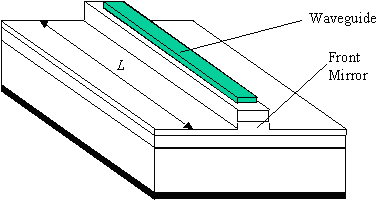 |
| Figure 4.10.1 : | Structure of an edge-emitting laser diode. |
The light in the waveguide is amplified by stimulated emission. Stimulated emission is a process where a photon triggers the radiative recombination of an electron and hole thereby creating an additional photon with the same energy and phase as the incident photon. This process is illustrated with Figure 4.10.2. This "cloning" of photons results in a coherent beam. |
 |
| Figure 4.10.2 : | Stimulated emission of a photon. |
The stimulated emission process yields an increase in photons as they travel along the waveguide. |
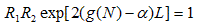
Combined with the waveguide losses, stimulated emission yields a net gain per unit length, g. The number of photons can therefore be maintained if the roundtrip amplification in a cavity of length, L, including the partial reflection at the mirrors with reflectivity R1 and R2 equals unity. |
This yields the following lasing condition: |
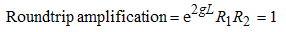 | (4.10.1) |
If the roundtrip amplification is less than one then the number of photons steadily decreases. If the roundtrip amplification is larger than one, the number of photons increases as the photons travel back and forth in the cavity and no steady state value would be obtained. The gain required for lasing therefore equals: |
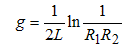 | (4.10.2) |
Initially, the gain is negative if no current is applied to the laser diode as absorption dominates in the waveguide. As the laser current is increased, the absorption first decreases and the gain increases. |
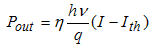
The current for which the gain satisfies the lasing condition is the threshold current of the laser, Ith. Below the threshold current very little light is emitted by the laser structure. For an applied current larger than the threshold current, the output power, Pout, increases linearly with the applied current as illustrated with Figure 4.10.4. The output power therefore equals: |
 | (4.10.3) |
where hn is the energy per photon. The factor, h, indicates that only a fraction of the generated photons contribute to the output power of the laser as photons are partially lost through the other mirror and throughout the waveguide. |
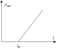 |
| Figure 4.10.3 : | Output power from a laser diode versus the applied current. |
4.10.2. Laser cavities and laser cavity modes | |
A laser diode consists of a cavity, defined as the region between two mirrors with reflectivity R1 and R2, and a gain medium, in our case a quantum well. The optical mode originates in spontaneous emission, which is confined to the cavity by the waveguide. This optical mode is amplified by the gain medium and partially reflected by the mirrors. The modal gain depends on the gain of the medium, multiplied with the overlap between the gain medium and the optical mode which we call the confinement factor, G, or: |
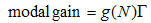 | (4.10.4) |
This confinement factor will be calculated in section 4.10.2. Lasing occurs when the round trip optical gain equals the losses. For a laser with modal gain g(N)G and waveguide loss, a, this condition implies: |
 | (4.10.5) |
where L is the length of the cavity. The distributed loss of the mirrors is therefore: |
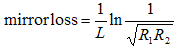 | (4.10.6) |
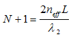
Longitudinal modes in the laser cavity correspond to standing waves between the mirrors. If we assume total reflection at the mirrors this wave contains N/2 periods where N is an integer. For a given wave length l and a corresponding effective index, neff, this yields: |
 | (4.10.7) |
Because of dispersion in the waveguide, a second order model should also include the wavelength dependence of the effective index. Ignoring such dispersion effects, we find the difference in wavelength between two adjacent longitudinal modes from: |
 | (4.10.8) |
 | (4.10.9) |
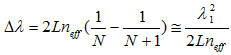 | (4.10.10) |
Longer cavities therefore have closer spaced longitudinal modes. An edge emitting (long) cavity with length of 300 mm, neff = 3.3, and l = 0.8 mm has a wavelength spacing Dl of 0.32 nm while a surface emitting (short) cavity of 3 mm has a wavelength spacing of only 32 nm. These wavelength differences can be converted to energy differences using: |
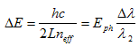 | (4.10.11) |
so that 0.32 nm corresponds to -6.2 meV and 32 nm to 620 meV. A typical width of the optical gain spectrum is 60 meV, so that an edge emitter biased below threshold can easily contain 10 longitudinal modes, while for a surface emitter the cavity must be carefully designed so that the longitudinal mode overlaps with the gain spectrum. |
A more detailed analysis of a Fabry-Perot etalon is described in Appendix 15, providing the reflectivity, absorption and transmission as a function of photon energy. |
The optical modes in the waveguide determine the effective index needed to calculate the longitudinal modes as well as the confinement factor. Starting from Maxwell's equations in the absence of sources: |
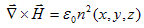 | (4.10.12) |
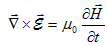 | (4.10.13) |
and assuming a propagating wave in the z-direction and no variation in the y-direction, we obtain the following one-dimensional reduced wave equation for a time harmonic field, |
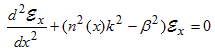 | (4.10.14) |
Where, b, is the propagation constant given by |
 | (4.10.15) |
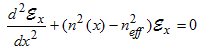
this equation is very similar to the Schr�dinger equation. In fact, previous solutions for quantum wells can be used to solve Maxwell's equation by setting the potential V(x) equal to -n2 (x) and replacing |
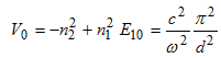 | (4.10.16) |
or, |
 | (4.10.17) |
For l = 0.8 mm, n1 = 3.5 and n2 = 3.3 one finds d � 0.34 mm. |
The confinement factor is defined as the ratio of the modal gain to the gain in the active medium at the wavelength of interest: |
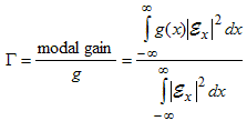 | (4.10.18) |
for a quantum well with width Lx, the confinement factor reduces to |
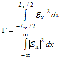 | (4.10.19) |
which is approximately @ 0.02...0.04 for a typical GaAs single quantum well laser |
4.10.3. Emission, Absorption and modal gain | |
The analysis of a semiconductor laser diode requires a detailed knowledge of the modal gain, which quantifies the amplification of light confined to the lasing mode. To find the modal gain, one starts from the requirement that the emission as well as absorption of photons, must conserve both energy and momentum of all particles involved in the process. The conservation of energy requires that the photon energy equals the difference between the electron and hole energy: |
 | (4.10.20) |
with |
 | (4.10.21) |
 | (4.10.22) |
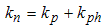
The conservation of momentum requires that the electron momentum equals that of the empty state it occupies in the valence band plus the momentum of the photon |
 | (4.10.23) |
The photon momentum is much smaller than that of the electron and hole, so that the electron and hole momentum are approximately equal. As a result we can replace kn and kp by a single variable k. Equations (4.10.20), (4.10.21), (4.10.22) and (4.10.23) then result in: |
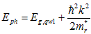 | (4.10.24) |
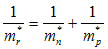
where Eg,qw1 is the energy between the lowest electron energy in the conduction band and the lowest hole energy in the valence band. mr* is the reduced effective mass given by: |
 | (4.10.25) |
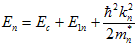
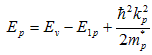
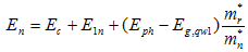
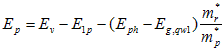
The electron and hole energies, En and Ep, can then be expressed as a function of the photon energy by: |
 | (4.10.26) |
 | (4.10.27) |
The emission and absorption spectra (b(Eph) and a(Eph)) of a quantum well depend on the density of states and the occupancy of the relevant states in the conduction and valence band. Since the density of states in the conduction and valence band is constant in a quantum well, the emission and absorption can be expressed as a product of a maximum emission and absorption rate and the probability of occupancy of the conduction and valence band states, namely: |
 | (4.10.28) |
 | (4.10.29) |
Stimulated emission occurs if an incoming photon triggers the emission of another photon. The net gain in the semiconductor is the stimulated emission minus the absorption. The maximum stimulated emission equals the maximum absorption since the initial and final states are simply reversed so that the transition rates as calculated based on the matrix elements are identical. The net gain is then given by: |
 | (4.10.30) |
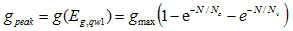
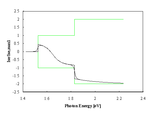
where the maximum stimulated emission and the maximum absorption were replaced by the maximum gain, gmax. The normalized gain spectrum is shown in Figure 4.10.4 for different values of the carrier density. The two staircase curves indicate the maximum possible gain and the maximum possible absorption in the quantum well. |
 |
| Figure 4.10.4: | Normalized gain versus photon energy of a 10nm GaAs quantum well for a carrier density of 1012 (lower curve), 3 x 10¹², 5 x 10¹², 7 x 10¹² and 9 x 10¹² (upper curve) cm-2. |
The theoretical gain curve of Figure 4.10.4 exhibits a sharp discontinuity at Eph = Eg,qw1. The gain can also be expressed as a function of the carrier densities, N and P, when assuming that only one electron and one hole level is occupied: |
 | (4.10.31) |
The peak value at Eph = Eg,qw1, assuming quasi-neutrality (N = P) is then: |
 | (4.10.32) |
The maximum gain can be obtained from the absorption of light in bulk material: One can verify that the wavefunction of a free electron in bulk material is the same as the wavefunction in an infinite stack of infinitely deep quantum wells, provided the barriers are infinitely thin and placed at the nodes of the wavefunction. This means that for such a set of quantum wells the absorption would be the same as in bulk provided that the density of states is also the same. This is the case for Eph = Eqw1, so that the maximum gain per unit length is given by: |
 | (4.10.33) |
where Lx is the width of the quantum well. This expression shows that the total gain of a single quantum well due to a single quantized level is independent of the width. The corresponding value for GaAs quantum wells is 0.006 or 0.6%. |
Experimental gain curves do not show the discontinuity at Eph = Eqw1 due to inter-carrier scattering which limits the lifetime of carriers in a specific state. The line width of a single set of electron and hole levels widens as a function of the scattering time, which disturbs the phase of the atomic oscillator. Therefore, an approximation to the actual gain curve can be obtained by convoluting (4.10.30) with a Lorenzian line shape function: |
 | (4.10.34) |
with |
 |
| Figure 4.10.5: | Original and convoluted gain spectrum of a 10 nm GaAs quantum well with a carrier density of 3 x 1012 cm-2 and a collision time of 0.09 ps. |
For lasers with long cavities such as edge-emitter lasers, one finds that the longitudinal modes are closely spaced so that lasing will occur at or close to the peak of the gain spectrum. It is therefore of interest to find an expression for the peak gain as a function of the carrier density. A numeric solution is shown in Figure 4.10.6 where the peak gain is normalized to the maximum value of the first quantized energy level. Initially, the gain peak is linear with carrier concentration but saturates because of the constant density of states, until the gain peak associated with the second quantized level takes over. Since the peak gain will be relevant for lasing, we will consider it more closely. As a first order approximation we will set the peak gain g(N) equal to: |
 | (4.10.35) |
where |
 | (4.10.36) |
 |
| Figure 4.10.6: | Calculated gain versus carrier density for a 10 nm GaAs quantum well (solid line) compared to equation (4.10.32) |
From Figure 4.10.6 one finds that the material becomes "transparent" when the gain equals zero or: |
 | (4.10.37) |
which can be solved yielding: |
 | (4.10.38) |
The transparency current density is defined as the minimal current density for which the material becomes transparent for any photon energy larger than or equal to Eg,qw1. This means that the transparency condition is fulfilled for |
 | (4.10.39) |
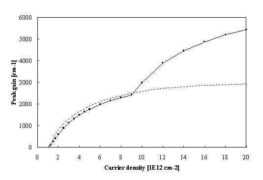
This expression can be solved by iteration for Nv > Nc. The solution is shown in Figure 4.10.7. |
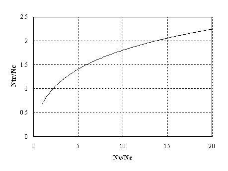 |
| Figure 4.10.7: | Normalized transparency carrier density versus the ratio of the effective density of states in the valence and conduction band. |
To include multiple hole levels one simply replaces Nv by Nv,qw* as described in section 4.3.8.6. |
4.10.4. The rate equations for a laser diode. | |
Rate equations for each longitudinal mode, l, with photon density Sl and carrier density Nl which couple into this mode are: |
 | (4.10.40) |
 | (4.10.41) |
Rather than using this set of differential equations for all waveguide modes, we will only consider one mode with photon density S, whose photon energy is closest to the gain peak. The intensity of this mode will grow faster than all others and eventually dominate. This simplification avoids the problem of finding the parameters and coefficients for every single mode. On the other hand it does not enable to calculate the emission spectrum of the laser diode. For a single longitudinal mode the rate equations reduce to: |
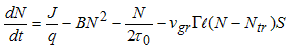 | (4.10.42) |
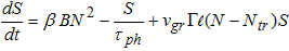 | (4.10.43) |
 | (4.10.44) |
The time independent rate equations, ignoring spontaneous emission, are: |
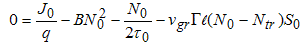 | (4.10.45) |
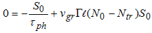 | (4.10.46) |
where the photon life time is given by: |
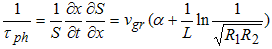 | (4.10.47) |
from which we can solve the carrier concentration while lasing: |
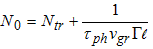 | (4.10.48) |
which is independent of the photon density. The threshold current density is obtained when S0 = 0 |
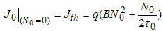 | (4.10.49) |
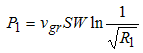
The photon density above lasing threshold, and power emitted through mirror R1, are given by: |
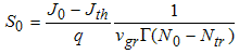 | (4.10.50) |
and the power emitted through mirror 1 is: |
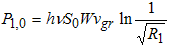 | (4.10.51) |
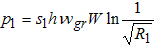
The differential efficiency of the laser diode is: |
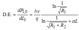 | (4.10.52) |
and the quantum efficiency is: |
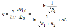 | (4.10.53) |
Efficient lasers are therefore obtained by reducing the waveguide losses, increasing the reflectivity of the back mirror, decreasing the reflectivity of the front mirror and decreasing the length of the cavity. Decreasing the reflectivity of the mirror also increases the threshold current and is therefore less desirable. Decreasing the cavity length at first decreases the threshold current but then rapidly increases the threshold current. |
Assuming a time-harmonic solution and ignoring higher order terms (as we did for the LED) the rate equations become: |
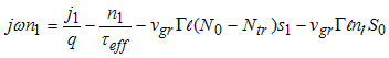 | (4.10.54) |
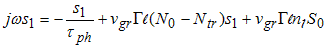 | (4.10.55) |
where teff is the same as for an LED and given by equation (4.9.21). Using |
 | (4.10.56) |
We now replace n1 by relating it to the small signal voltage v1: |
 | (4.10.57) |
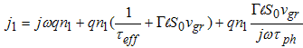
The equation for the small signal current, I1, can be then written as |
 | (4.10.58) |
with |
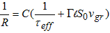 | (4.10.59) |
and |
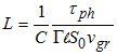 | (4.10.60) |
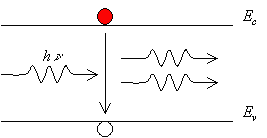
Adding parasitic elements and the circuit described by the equation (4.10.58) we obtain the equivalent circuit of Figure 4.10.8, where LB is a series inductance, primarily due to the bond wire, Rs is the series resistance in the device and Cp is the parallel capacitance due to the laser contact and bonding pad. |
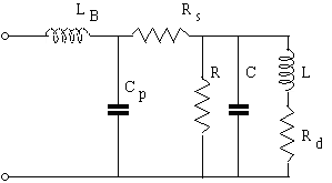 |
| Figure 4.10.8: | Small signal equivalent circuit of a laser diode |
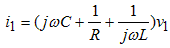
The resistor, Rd, in series with the inductor, L, is due to gain saturation and can be obtained by adding a gain saturation term to equation (4.10.35). The optical output power is proportional to the current through inductor L, i1,L, which is given by: |
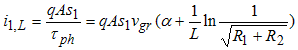 | (4.10.61) |
and the corresponding power emitted from mirror R1 |
 | (4.10.62) |
When further ignoring the parasitic elements and the gain saturation resistance, Rd, one finds the ac responsivity p1/I1 as: |
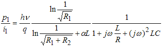 | (4.10.63) |
from which we find the relaxation frequency of the laser: |
 | (4.10.64) |
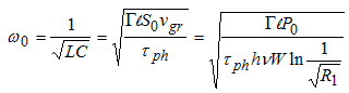
The relaxation frequency is therefore proportional to the square root of the DC output power. The amplitude at the relaxation frequency relative to that at zero frequency equals: |
 | (4.10.65) |
4.10.5. Large signal switching of a laser diode | |
Because of the non-linear terms in the rate equations the large signal switching of a laser diode exhibits some peculiar characteristics. The response to a current step is shown in the Figure 4.10.1. The carrier density initially increases linearly with time while the photon density remains very small since stimulated emission only kicks in for N > N0. |
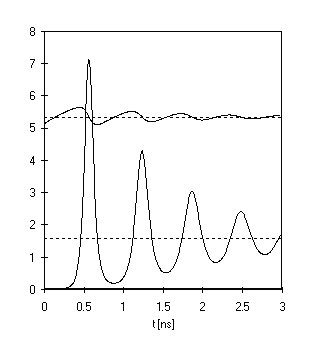 |
| Figure 4.10.9: | Optical power and normalized carrier concentration versus time when applying a step current at t = 0 from I = 0.95 Ith to I = 1.3 Ith. |
Both the carrier density and the photon density oscillate around their final value. The oscillation peaks are spaced by roughly 2p/w0, where w0 is the small signal relaxation frequency at the final current. The photon and carrier densities are out of phase as carriers are converted into photons due to stimulated emission, while photons are converted back into electron-hole pairs due to absorption. One can use the non-linear behavior to generate short optical pulses. By applying a current pulse, which is long enough to initiate the first peak in the oscillation, but short enough to avoid the second peak, one obtains a single optical pulse, which is significantly shorter that the applied current pulse. This method is referred to as gain switching or current spiking. |
 =
=  , and
, and  . The equation then becomes:
 by
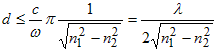
by  . The energy eigenvalues, El, can then be interpreted as minus the effective indices of the modes: -n2eff,l. One particular waveguide of interest is a slab waveguide consisting of a piece of high refractive index material, n1, with thickness d, between two infinitely wide cladding layers consisting of lower refractive index material, n2. From Appendix 17 one finds that only one mode exists for:
 , where t is the carrier collision time in the quantum well. The original and convoluted gain curves are shown in Figure
  is the differential gain coefficient. This approximation is only valid close to N = Ntr, and even more so for quantum well lasers as opposed to double-hetero-structure lasers. An approximate value for the differential gain coefficient of a quantum well can be calculated from (
 . The corresponding carrier density is referred to as Ntr, the transparency carrier density. The transparency carrier density can be obtained from by setting gmax = 0, yielding
 these equations can be solved yielding:
 , and
, and  , where A is the area of the laser diode.