In this section we summarize the calculation of the threshold voltage and discuss the dependence of the threshold voltage on the bias applied to the substrate, called the substrate bias effect. |
7.4.1. Threshold voltage calculation |   |
The threshold voltage equals the sum of the flatband voltage, twice the bulk potential and the voltage across the oxide due to the depletion layer charge, or: |
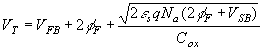 | (7.4.1) |
where the flatband voltage, VFB, is given by: |
 | (7.4.2) |
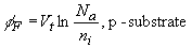
With |
 | (7.4.3) |
and |
 | (7.4.4) |
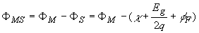
The threshold voltage of a p-type MOSFET with an n-type substrate is obtained using the following equations: |
 | (7.4.5) |
where the flatband voltage, VFB, is given by: |
 | (7.4.6) |
With |
 | (7.4.7) |
and |
 | (7.4.8) |
The threshold voltage dependence on the doping density is illustrated with Figure 7.4.1 for both n-type and p-type MOSFETs with an aluminum gate metal. |
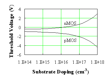 |
| Figure 7.4.1 : | Threshold voltage of n-type (upper curve) and p-type (lower curve) MOSFETs versus substrate doping density.  |
The threshold of both types of devices is slightly negative at low doping densities and differs by 4 times the absolute value of the bulk potential. The threshold of nMOSFETs increases with doping while the threshold of pMOSFETs decreases with doping in the same way. A variation of the flatband voltage due to oxide charge will cause a reduction of both threshold voltages if the charge is positive and an increase if the charge is negative. |
7.4.2. The substrate bias effect | |
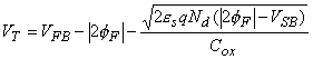
The voltage applied to the back contact affects the threshold voltage of a MOSFET. The voltage difference between the source and the bulk, VBS changes the width of the depletion layer and therefore also the voltage across the oxide due to the change of the charge in the depletion region. This results in a modified expression for the threshold voltage, as given by: |
 | (7.4.9) |
The threshold difference due to an applied source-bulk voltage can therefore be expressed by: |
 | (7.4.10) |
Where Γ is the body effect parameter given by: |
 | (7.4.11) |
The variation of the threshold voltage with the applied bulk-to-source voltage can be observed by plotting the transfer curve for different bulk-to-source voltages. The expected characteristics, as calculated using the quadratic model and the variable depletion layer model, are shown in Figure 7.4.2. |
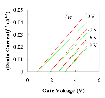 |
| Figure 7.4.2 : | Square root of ID versus the gate-source voltage as calculated using the quadratic model (upper curves) and the variable depletion layer model (lower curves). |
First, we observe that the threshold shift is the same for both models. For a device biased at the threshold voltage, drain saturation is obtained at zero drain-to-source voltage so that the depletion layer width is constant along the channel. As the drain-source voltage at saturation is increased, there is an increasing difference between the drain current as calculated with each model. The difference however reduces as a more negative bulk-source voltage is applied. This is due to the larger depletion layer width, which reduces the relative variation of the depletion layer charge along the channel. |
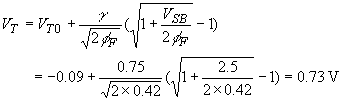
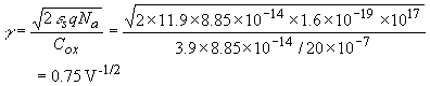
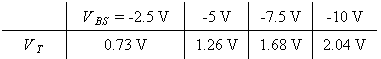
| Example 7.3 | Calculate the threshold voltage of a silicon nMOSFET when applying a substrate voltage, VBS = 0, -2.5, -5, -7.5 and -10 V. The capacitor has a substrate doping Na = 1017 cm-3, a 20 nm thick oxide (εox = 3.9 ε0) and an aluminum gate (ΦM = 4.1 V). Assume there is no fixed charge in the oxide or at the oxide-silicon interface. |
| Solution | The threshold voltage at VBS = -2.5 V equals:
|
Boulder, December 2004 |